Manufacturing method for composite alloy bonding wire
US20100319872A1
2010-12-23
12/869,854
2010-08-27
✅ Patent granted
US 8,101,030 B2
2012-01-24
-
-
Emily Le | Rebecca Lee
2030-08-27
Abstract:
A manufacturing method for a composite alloy bonding wire is provided. A primary material of Au and Ag is melted in a vacuum melting furnace, and then a secondary metal material of Pd is added into the vacuum melting furnace and is co-melted with the primary material to obtain a Au-Ag-Pd alloy solution. The obtained Au-Ag-Pd alloy solution is drawn to obtain a Au-Ag-Pd alloy wire. The Au-Ag-Pd alloy wire is then drawn to obtain a Au-Ag-Pd alloy bonding wire with a predetermined diameter.
Interested in similar patents?
Get notified when new applications in this technology area are published.
Classification:
B21C1/003 » CPC further
Manufacture of metal sheets, metal wire, metal rods, metal tubes by drawing Drawing materials of special alloys so far as the composition of the alloy requires or permits special drawing methods or sequences
B21C37/047 » CPC further
Manufacture of metal sheets, bars, wire, tubes or like semi-manufactured products, not otherwise provided for; Manufacture of tubes of special shape of bars or wire of fine wires
B23K35/0261 » CPC further
Rods, electrodes, materials, or media, for use in soldering, welding, or cutting characterised by mechanical features, e.g. shape for use in welding Rods, electrodes, wires
B23K35/24 » CPC further
Rods, electrodes, materials, or media, for use in soldering, welding, or cutting characterised by the composition or nature of the material Selection of soldering or welding materials proper
B23K35/3006 » CPC further
Rods, electrodes, materials, or media, for use in soldering, welding, or cutting characterised by the composition or nature of the material; Selection of soldering or welding materials proper with the principal constituent melting at less than 1550 degrees C Ag as the principal constituent
C22C1/02 » CPC further
Making alloys by melting
C22F1/14 » CPC further
Changing the physical structure of non-ferrous metals or alloys by heat treatment or by hot or cold working of noble metals or alloys based thereon
H01L24/43 » CPC further
Arrangements for connecting or disconnecting semiconductor or solid-state bodies; Methods or apparatus related thereto; Means for bonding being attached to, or being formed on, the surface to be connected, e.g. chip-to-package, die-attach, "first-level" interconnects; Manufacturing methods related thereto; Wire connectors; Manufacturing methods related thereto Manufacturing methods
H01L24/45 » CPC further
Arrangements for connecting or disconnecting semiconductor or solid-state bodies; Methods or apparatus related thereto; Means for bonding being attached to, or being formed on, the surface to be connected, e.g. chip-to-package, die-attach, "first-level" interconnects; Manufacturing methods related thereto; Wire connectors; Manufacturing methods related thereto; Structure, shape, material or disposition of the wire connectors prior to the connecting process of an individual wire connector
H01L2224/43 » CPC further
Indexing scheme for arrangements for connecting or disconnecting semiconductor or solid-state bodies and methods related thereto as covered by; Means for bonding being attached to, or being formed on, the surface to be connected, e.g. chip-to-package, die-attach, "first-level" interconnects; Manufacturing methods related thereto; Wire connectors; Manufacturing methods related thereto Manufacturing methods
H01L2924/01027 » CPC further
Indexing scheme for arrangements or methods for connecting or disconnecting semiconductor or solid-state bodies as covered by; Chemical elements Cobalt [Co]
H01L2924/01029 » CPC further
Indexing scheme for arrangements or methods for connecting or disconnecting semiconductor or solid-state bodies as covered by; Chemical elements Copper [Cu]
H01L2924/01047 » CPC further
Indexing scheme for arrangements or methods for connecting or disconnecting semiconductor or solid-state bodies as covered by; Chemical elements Silver [Ag]
H01L2924/14 » CPC further
Indexing scheme for arrangements or methods for connecting or disconnecting semiconductor or solid-state bodies as covered by; Details of semiconductor or other solid state devices to be connected; Device type Integrated circuits
H01L2924/01079 » CPC further
Indexing scheme for arrangements or methods for connecting or disconnecting semiconductor or solid-state bodies as covered by; Chemical elements Gold [Au]
H01L2924/01046 » CPC further
Indexing scheme for arrangements or methods for connecting or disconnecting semiconductor or solid-state bodies as covered by; Chemical elements Palladium [Pd]
H01L2924/20755 » CPC further
Indexing scheme for arrangements or methods for connecting or disconnecting semiconductor or solid-state bodies as covered by; Parameters; Diameter ranges larger or equal to 50 microns less than 60 microns
C22C5/06 » CPC main
Alloys based on noble metals Alloys based on silver
H01L2924/20754 » CPC further
Indexing scheme for arrangements or methods for connecting or disconnecting semiconductor or solid-state bodies as covered by; Parameters; Diameter ranges larger or equal to 40 microns less than 50 microns
H01L2924/20753 » CPC further
Indexing scheme for arrangements or methods for connecting or disconnecting semiconductor or solid-state bodies as covered by; Parameters; Diameter ranges larger or equal to 30 microns less than 40 microns
H01L2924/20752 » CPC further
Indexing scheme for arrangements or methods for connecting or disconnecting semiconductor or solid-state bodies as covered by; Parameters; Diameter ranges larger or equal to 20 microns less than 30 microns
H01L2924/20751 » CPC further
Indexing scheme for arrangements or methods for connecting or disconnecting semiconductor or solid-state bodies as covered by; Parameters; Diameter ranges larger or equal to 10 microns less than 20 microns
H01L2924/013 » CPC further
Indexing scheme for arrangements or methods for connecting or disconnecting semiconductor or solid-state bodies as covered by Alloys
H01L2224/48 » CPC further
Indexing scheme for arrangements for connecting or disconnecting semiconductor or solid-state bodies and methods related thereto as covered by; Means for bonding being attached to, or being formed on, the surface to be connected, e.g. chip-to-package, die-attach, "first-level" interconnects; Manufacturing methods related thereto; Wire connectors; Manufacturing methods related thereto; Structure, shape, material or disposition of the wire connectors after the connecting process of an individual wire connector
H01L2924/12041 » CPC further
Indexing scheme for arrangements or methods for connecting or disconnecting semiconductor or solid-state bodies as covered by; Details of semiconductor or other solid state devices to be connected; Device type; Passive devices, e.g. 2 terminal devices; Optical Diode LED
H01L2924/00 » CPC further
Indexing scheme for arrangements or methods for connecting or disconnecting semiconductor or solid-state bodies as covered by
H01L2924/01049 » CPC further
Indexing scheme for arrangements or methods for connecting or disconnecting semiconductor or solid-state bodies as covered by; Chemical elements Indium [In]
H01L2924/01006 » CPC further
Indexing scheme for arrangements or methods for connecting or disconnecting semiconductor or solid-state bodies as covered by; Chemical elements Carbon [C]
H01L2224/43848 » CPC further
Indexing scheme for arrangements for connecting or disconnecting semiconductor or solid-state bodies and methods related thereto as covered by; Means for bonding being attached to, or being formed on, the surface to be connected, e.g. chip-to-package, die-attach, "first-level" interconnects; Manufacturing methods related thereto; Wire connectors; Manufacturing methods related thereto; Manufacturing methods; Post-treatment of the connector Thermal treatments, e.g. annealing, controlled cooling
H01L2924/00014 » CPC further
Indexing scheme for arrangements or methods for connecting or disconnecting semiconductor or solid-state bodies as covered by; Technical content checked by a classifier the subject-matter covered by the group, the symbol of which is combined with the symbol of this group, being disclosed without further technical details
H01L2924/00011 » CPC further
Indexing scheme for arrangements or methods for connecting or disconnecting semiconductor or solid-state bodies as covered by; Technical content checked by a classifier Not relevant to the scope of the group, the symbol of which is combined with the symbol of this group
H01L2924/01005 » CPC further
Indexing scheme for arrangements or methods for connecting or disconnecting semiconductor or solid-state bodies as covered by; Chemical elements Boron [B]
B22D25/02 IPC
Special casting characterised by the nature of the product by its peculiarity of shape; of works of art
B22D27/00 IPC
Treating the metal in the mould while it is molten or ductile Pressure or vacuum casting
C22F1/00 IPC
Changing the physical structure of non-ferrous metals or alloys by heat treatment or by hot or cold working
Description
This application is a divisional application of U.S. patent application Ser. No. 12/408,987, filed on Mar. 23, 2009.
BACKGROUND OF THE INVENTION
1. Field of the Invention
The present invention generally relates to a bonding wire used as a packaging wire, in particular, to a bonding wire used in semiconductor packaging process.
2. Description of Related Art
In semiconductor device packaging processes for IC, LED, SAW, a wire bonding process is often performed to electrically connect the chip to the substrate by bonding wire, which used as a signal and electrical current transmitting medium between the chip and the substrate.
The primary characteristics of a bonding wire, such as breaking load, elongation, loop, melting point, and bondability with IC chips are dependent on the materials used as the bonding wire. The performance of the packaged semiconductor device is influenced by the characteristics of the bonding wire. According to different types of chip and substrate, the adapted bonding wire has different specification.
The conventional bonding wires are usually made of pure Au material. Pure Au bonding wire has better physical properties, such as elongation and electrical conductivity. However, pure Au bonding wire inevitably leads to high cost.
Therefore, the subject of the present invention is to solve the above mentioned problem to provide a low cost bonding wire with performance comparable to pure Au bonding wire.
SUMMARY OF THE INVENTION
The subject of this invention is to provide a low cost composite alloy bonding wire made of Gold, silver and Palladium, capable of having performance as good as a pure Au bonding wire.
In order to obtain the above mentioned subject, a manufacturing method for a composite alloy bonding wire is disclosed. A primary metal material of Au and Ag is melted in a vacuum melting furnace, and then a secondary metal material of Pd is added into the vacuum melting furnace and is co-melted with the primary metal material to obtain a Au-Ag-Pd alloy solution. The obtained Au-Ag-Pd alloy solution is then cast and drawn to obtain a Au-Ag-Pd alloy wire. Finally, the obtained Au-Ag-Pd alloy wire is then drawn to obtain a Au-Ag-Pd alloy bonding wire with a predetermined diameter.
Besides, a composite alloy bonding wire made by the abovementioned manufacturing method is provided. The composite alloy bonding wire includes 8.00˜30.00 wt. % Au, 66.00˜90.00 wt. % Ag and 0.01˜6.00 wt. % Pd.
The composite alloy bonding wire is capable of having performance as good as a pure Au bonding wire and decreasing the manufacturing cost.
BRIEF DESCRIPTION OF DRAWING
The features of the invention believed to be novel are set forth with particularity in the appended claims. The invention itself, however, may be best understood by reference to the following detailed description of the invention, which describes an exemplary embodiment of the invention, taken in conjunction with the accompanying drawings, in which:
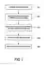
FIG. 1 is a flow chart for manufacturing composite alloy bonding wire of the present invention; and
FIG. 2 shows detailed sub-steps in the flow chart of FIG. 1.
DETAILED DESCRIPTION OF THE INVENTION
In cooperation with attached drawings, the technical contents and detailed description of the present invention are described thereinafter according to a preferable embodiment, being not used to limit its executing scope. Any equivalent variation and modification made according to appended claims is all covered by the claims claimed by the present invention.
Refer to FIG. 1 and FIG. 2, which respectively are a flow chart for manufacturing composite alloy bonding wire of the present invention and a drawing showing detailed sub-steps in the flow chart of FIG. 1. Step 100, a primary material of Au and Ag is provided.
Step 102, the primary material is melted in a vacuum melting furnace (step 102a). Specific amount of a secondary metal material of Pd is added into the vacuum melting furnace (step 102b), and co-melted with the primary material in the vacuum melting furnace to obtain a Au-Ag-Pd alloy solution (step 102c). The Au-Ag-Pd alloy solution consists of 8.00˜30.00 wt. % Au, 66.00˜90.00 wt. % Ag and 0.01˜6.00 wt. % Pd.
Subsequently, continuous casting and drawing processes are performed on the Au-Ag-Pd alloy solution to obtain a Au-Ag-Pd alloy wire with diameter of 4-8 mm (step 102d). The Au-Ag-Pd alloy wire is rewired by a reeling machine (step 102e) and then composition analysis (102f) is performed on the Au-Ag-Pd alloy wire to check if the obtained composition meets the requirement.
Step 104, a drawing process is performed on the Au-Ag-Pd alloy wire; the obtained Au-Ag-Pd alloy wire with a diameter of 4-8 mm is drawn by a first thick drawing machine to obtain a Au-Ag-Pd alloy wire with a diameter of 3 mm or smaller than 3 mm (step 104a). The Au-Ag-Pd alloy wire with a diameter of 3 mm or smaller than 3 mm is drawn by a second thick drawing machine to obtain a Au-Ag-Pd alloy wire with a predetermined diameter of 1 mm or smaller than 1 mm (step 104b). The Au-Ag-Pd alloy wire with diameter 1 mm or smaller than 1 mm is drawn by a first thin drawing machine to obtain a Au-Ag-Pd alloy wire with a diameter of 0.18 mm or smaller than 0.18 mm (step 104c). Then the Au-Ag-Pd alloy wire with a diameter of 0.18 mm or smaller than 0.18 mm is sequentially drawn by the second thin drawing machine (step 104d), a very thin drawing machine (step 104e) and an ultra thin drawing machine (step 104f) to obtain an ultra thin Au-Ag-Pd alloy bonding wire with a predetermined diameter of 0.050 mm (2.00 mil) to 0.010 mm (0.40 mil).
Step 106, the surface of the Au-Ag-Pd alloy bonding wire is cleaned.
Step 108, the Au-Ag-Pd alloy bonding wire is annealed to ensure a final product with desirable physical properties of breaking load and elongation.
The Au-Ag-Pd alloy bonding wire can be applied to packaging process of IC, LED and SAW.
The invention is more detailed described by three embodiments below:
Embodiment 1
A primary material of Au and Ag is provided and is melted in a vacuum melting furnace. Then, specific amount of a secondary metal material of Pd is added into the vacuum melting furnace, and is co-melted with the primary material in the vacuum melting furnace to obtain a Au-Ag-Pd alloy solution. The Au-Ag-Pd alloy solution consists of: 30.00 wt. % Au, 66.00 wt. % Ag and 4.00 wt. % Pd.
Continuous casting and drawing processes are performed on the Au-Ag-Pd alloy solution to obtain a Au-Ag-Pd alloy wire with a diameter of 4 mm. The Au-Ag-Pd alloy wire is rewired by a reeling machine and then composition analysis is performed on the Au-Ag-Pd alloy wire to check if the obtained composition meets the requirement.
A drawing process is performed on the Au-Ag-Pd alloy wire; the obtained Au-Ag-Pd alloy wire with a diameter of 4 mm is drawn by a first thick drawing machine to obtain a Au-Ag-Pd alloy wire with a diameter of 3 mm. The Au-Ag-Pd alloy wire with a diameter of 3 mm is drawn by a second thick drawing machine to obtain a Au-Ag-Pd alloy wire with a diameter of 1 mm. The Au-Ag-Pd alloy wire with a diameter of 1 mm is drawn by a first thin drawing machine to obtain a Au-Ag-Pd alloy wire with a diameter of 0.18 mm. Then the Au-Ag-Pd alloy wire with a diameter of 0.18 mm is sequentially drawn by the second thin drawing machine, a very thin drawing machine and an ultra thin drawing machine to obtain an ultra thin Au-Ag-Pd alloy bonding wire with a predetermined diameter of 0.050 mm to 0.010 mm.
Finally, the surface of Au-Ag-Pd alloy bonding wire is cleaned and is annealed.
Embodiment 2
A primary material of Au and Ag is provided and is melted in a vacuum melting furnace. Then, specific amount of a secondary metal material of Pd is added into the vacuum melting furnace, and is co-melted with the primary material in the vacuum melting furnace to obtain a Au-Ag-Pd alloy solution. The Au-Ag-Pd alloy solution consists of 8.00 wt. % Au, 86.00 wt. % Ag and 6.00 wt. % Pd.
Continuous casting and drawing processes are performed on the Au-Ag-Pd alloy solution to obtain a Au-Ag-Pd alloy wire with a diameter of 6 mm. The Au-Ag-Pd alloy wire is rewired by a reeling machine and then composition analysis is performed on the Au-Ag-Pd alloy wire to check if the obtained composition meets the requirement.
A drawing process is performed on the Au-Ag-Pd alloy wire; the obtained Au-Ag-Pd alloy wire with a diameter of 6 mm is drawn by a first thick drawing machine to obtain a Au-Ag-Pd alloy wire with a diameter of 3 mm. The Au-Ag-Pd alloy wire with a diameter of 3 mm is drawn by a second thick drawing machine to obtain a Au-Ag-Pd alloy wire with a diameter of 1.0 mm. The Au-Ag-Pd alloy wire with a diameter of 1.0 mm is drawn by a first thin drawing machine to obtain a Au-Ag-Pd alloy wire with a diameter of 0.18 mm. Then the Au-Ag-Pd alloy wire with a diameter of 0.18 mm is sequentially drawn by the second thin drawing machine, a very thin drawing machine and an ultra thin drawing machine to obtain an ultra thin Au-Ag-Pd alloy bonding wire with a predetermined diameter of 0.050 mm to 0.010 mm.
Finally, the surface of Au-Ag-Pd alloy bonding wire is cleaned and is annealed.
Embodiment 3
A primary material of Au and Ag is provided and is melted in a vacuum melting furnace. Then, specific amount of a secondary metal material of Pd is added into the vacuum melting furnace, and is co-melted with the primary material in the vacuum melting furnace to obtain a Au-Ag-Pd alloy solution. The Au-Ag-Pd alloy solution consists of 9.99 wt. % Au, 90.00 wt. % Ag and 0.01 wt. % Pd.
Continuous casting and drawing processes are performed on the Au-Ag-Pd solution to obtain a Au-Ag-Pd alloy wire with a diameter of 8 mm. The Au-Ag-Pd alloy wire is rewired by a reeling machine and then composition analysis is performed on the Au-Ag-Pd alloy wire to check if the obtained composition meets the requirement.
A drawing process is performed on the Au-Ag-Pd alloy wire; the obtained Au-Ag-Pd alloy wire with a diameter of 8 mm is drawn by a first thick drawing machine to obtain a Au-Ag-Pd alloy wire with a diameter of 2 mm. The Au-Ag-Pd alloy wire with a diameter of 2 mm is drawn by a second thick drawing machine to obtain a Au-Ag-Pd alloy wire with a diameter of 1.0 mm. The Au-Ag-Pd alloy wire with a diameter of 1.0 mm is drawn by a first thin drawing machine to obtain a Au-Ag-Pd alloy wire with a diameter of 0.18 mm. Then the Au-Ag-Pd alloy wire with a diameter of 0.18 mm is sequentially drawn by the second thin drawing machine, a very thin drawing machine and an ultra thin drawing machine to obtain an ultra thin Au-Ag-Pd alloy bonding wire with a predetermined diameter of 0.050 mm to 0.010 mm.
Finally, the surface of Au-Ag-Pd alloy bonding wire is cleaned and is annealed.
While the invention is described in by way of examples and in terms of preferred embodiments, it is to be understood that the invention is not limited thereto. On the contrary, the aim is to cover all modifications, alternatives and equivalents falling within the spirit and scope of the invention as defined by the appended claims.
Claims
What is claimed is:1. A manufacturing method for a composite alloy bonding wire, comprising:
a) providing a primary material of Au and Ag;
b) melting the primary material in a vacuum melting furnace, adding a secondary metal material of Pd into the vacuum melting furnace and co-melting with the primary material in the vacuum melting furnace to obtain a Au-Ag-Pd alloy solution;
c) casting and drawing the Au-Ag-Pd alloy solution to obtain a Au-Ag-Pd alloy wire; and
d) drawing the Au-Ag-Pd alloy wire to obtain a Au-Ag-Pd alloy bonding wire with a predetermined diameter.
2. The manufacturing method according to claim 1, wherein the weight percent of Au in step a) is 8.00%˜30.00%.
3. The manufacturing method according to claim 2, wherein the weight percent of Ag in step a) is 66.00%˜90.00%.
4. The manufacturing method according to claim 3, wherein the weight percent of Pd in step b) is 0.01%˜6.00%.
5. The manufacturing method according to claim 1, wherein the surface of the Au-Ag-Pd alloy bonding wire is cleaned and is annealed after step d).
Images & Drawings included:


Sources:
- United States Patent and Trademark Office - verify current appl. status at the USPTO↗
Similar patent applications:
Recent applications in this class:
- » 20220220580 2022-07-14
CONTACT MATERIAL MAINLY COMPOSED OF AG ALLOY, CONTACT USING THE CONTACT MATERIAL, AND ELECTRICAL DEVICE - » 20220119918 2022-04-21
Silver article - » 20210324497 2021-10-21
Thermally Stable Silver Alloy Coatings - » 20210115534 2021-04-22
Silver article and method for producing silver article - » 20190345583 2019-11-14
Sliding contact material and method for producing same - » 20190003015 2019-01-03
Age-hardenable sterling silver alloy with improved “tarnishing” resistance and master alloy composition for its production - » 20170335434 2017-11-23
Silver nanoparticle method on zinc oxide films - » 20170166999 2017-06-15
SILVER-ALLOY BASED SPUTTERING TARGET - » 20160376684 2016-12-29
SILVER ALLOY MATERIAL AND METHOD FOR MANUFACTURING THE SILVER ALLOY MATERIAL - » 20140369884 2014-12-18
AG ALLOY FILM TO BE USED AS REFLECTING FILM AND/OR TRANSMITTING FILM OR AS ELECTRICAL WIRING AND/OR ELECTRODE, AG ALLOY SPUTTERING TARGET, AND AG ALLOY FILLER