High bond line thickness for semiconductor devices
US20110037153A1
2011-02-17
12/887,821
2010-09-22
✅ Patent granted
US 9,147,665 B2
2015-09-29
-
-
Earl Taylor
Kenneth E. Horton | Kirton McConkie
2030-09-22
Abstract:
Die attach methods used in making semiconductor devices and the semiconductor devices resulting from those methods are described. The methods include providing a leadframe with a die attach pad, using a boundary feature(s) containing a bond wire to define a perimeter on the die attach pad, depositing a conductive material (such as solder) within the perimeter, and then attaching a die containing an integrated circuit device to the die attach pad by using the conductive material. The boundary feature(s) allow an increased thickness of conductive material to be used, resulting in increased bond line thickness and increasing the durability and performance of the resulting semiconductor package. Other embodiments are described.
Inventors:
- Yi LI 5 🇨🇳 Suzhou, China
- Zhengyu Zhu 1 🇨🇳 Suzhou City, China
- Yi Li 2 🇨🇳 Suzhou City, China
- FangFang Yang 2 🇨🇳 Suzhou City, China
- Zhengyu Zhu 2 🇨🇳 Suzhou, China
- FangFang Yang 2 🇨🇳 Suzhou, China
Assignee:
- FAIRCHILD SEMICONDUCTOR CORPORATION 389 🇺🇸 San Jose, CA, United States
Applicant:
Interested in similar patents?
Get notified when new applications in this technology area are published.
Classification:
H01L23/49513 » CPC further
Details of semiconductor or other solid state devices; Arrangements for conducting electric current to or from the solid state body in operation, e.g. leads, terminal arrangements ; Selection of materials therefor consisting of soldered constructions; Lead-frames or other flat leads characterised by the die pad having bonding material between chip and die pad
H01L2224/83 » CPC further
Indexing scheme for arrangements for connecting or disconnecting semiconductor or solid-state bodies and methods related thereto as covered by; Methods for connecting semiconductor or other solid state bodies using means for bonding being attached to, or being formed on, the surface to be connected using a layer connector
H01L24/83 » CPC further
Arrangements for connecting or disconnecting semiconductor or solid-state bodies; Methods or apparatus related thereto; Methods for connecting semiconductor or other solid state bodies using means for bonding being attached to, or being formed on, the surface to be connected using a layer connector
H01L24/97 » CPC further
Arrangements for connecting or disconnecting semiconductor or solid-state bodies; Methods or apparatus related thereto; Batch processes at chip-level, i.e. with connecting carried out on a plurality of singulated devices, i.e. on diced chips the devices being connected to a common substrate, e.g. interposer, said common substrate being separable into individual assemblies after connecting
H01L24/29 » CPC further
Arrangements for connecting or disconnecting semiconductor or solid-state bodies; Methods or apparatus related thereto; Means for bonding being attached to, or being formed on, the surface to be connected, e.g. chip-to-package, die-attach, "first-level" interconnects; Manufacturing methods related thereto; Layer connectors, e.g. plate connectors, solder or adhesive layers; Manufacturing methods related thereto; Structure, shape, material or disposition of the layer connectors prior to the connecting process of an individual layer connector
H01L24/48 » CPC further
Arrangements for connecting or disconnecting semiconductor or solid-state bodies; Methods or apparatus related thereto; Means for bonding being attached to, or being formed on, the surface to be connected, e.g. chip-to-package, die-attach, "first-level" interconnects; Manufacturing methods related thereto; Wire connectors; Manufacturing methods related thereto; Structure, shape, material or disposition of the wire connectors after the connecting process of an individual wire connector
H01L2224/26175 » CPC further
Indexing scheme for arrangements for connecting or disconnecting semiconductor or solid-state bodies and methods related thereto as covered by; Means for bonding being attached to, or being formed on, the surface to be connected, e.g. chip-to-package, die-attach, "first-level" interconnects; Manufacturing methods related thereto; Layer connectors, e.g. plate connectors, solder or adhesive layers; Manufacturing methods related thereto; Auxiliary members for layer connectors, e.g. spacers being formed on an item to be connected not being a semiconductor or solid-state body Flow barriers
H01L2224/83051 » CPC further
Indexing scheme for arrangements for connecting or disconnecting semiconductor or solid-state bodies and methods related thereto as covered by; Methods for connecting semiconductor or other solid state bodies using means for bonding being attached to, or being formed on, the surface to be connected using a layer connector; Pre-treatment of the layer connector or the bonding area Forming additional members, e.g. dam structures
H01L2224/8385 » CPC further
Indexing scheme for arrangements for connecting or disconnecting semiconductor or solid-state bodies and methods related thereto as covered by; Methods for connecting semiconductor or other solid state bodies using means for bonding being attached to, or being formed on, the surface to be connected using a layer connector; Bonding techniques using a polymer adhesive, e.g. an adhesive based on silicone, epoxy, polyimide, polyester
H01L2224/92 » CPC further
Indexing scheme for arrangements for connecting or disconnecting semiconductor or solid-state bodies and methods related thereto as covered by; Methods for connecting semiconductor or solid state bodies including different methods provided for in two or more of groups - Specific sequence of method steps
H01L2924/01005 » CPC further
Indexing scheme for arrangements or methods for connecting or disconnecting semiconductor or solid-state bodies as covered by; Chemical elements Boron [B]
H01L2924/01006 » CPC further
Indexing scheme for arrangements or methods for connecting or disconnecting semiconductor or solid-state bodies as covered by; Chemical elements Carbon [C]
H01L2924/01013 » CPC further
Indexing scheme for arrangements or methods for connecting or disconnecting semiconductor or solid-state bodies as covered by; Chemical elements Aluminum [Al]
H01L2924/01029 » CPC further
Indexing scheme for arrangements or methods for connecting or disconnecting semiconductor or solid-state bodies as covered by; Chemical elements Copper [Cu]
H01L2924/01033 » CPC further
Indexing scheme for arrangements or methods for connecting or disconnecting semiconductor or solid-state bodies as covered by; Chemical elements Arsenic [As]
H01L2924/01075 » CPC further
Indexing scheme for arrangements or methods for connecting or disconnecting semiconductor or solid-state bodies as covered by; Chemical elements Rhenium [Re]
H01L2924/01078 » CPC further
Indexing scheme for arrangements or methods for connecting or disconnecting semiconductor or solid-state bodies as covered by; Chemical elements Platinum [Pt]
H01L2924/078 » CPC further
Indexing scheme for arrangements or methods for connecting or disconnecting semiconductor or solid-state bodies as covered by; Polymers Adhesive characteristics other than chemical
H01L2924/0781 » CPC further
Indexing scheme for arrangements or methods for connecting or disconnecting semiconductor or solid-state bodies as covered by; Polymers; Adhesive characteristics other than chemical being an ohmic electrical conductor
H01L2924/07802 » CPC further
Indexing scheme for arrangements or methods for connecting or disconnecting semiconductor or solid-state bodies as covered by; Polymers; Adhesive characteristics other than chemical not being an ohmic electrical conductor
H01L2924/10329 » CPC further
Indexing scheme for arrangements or methods for connecting or disconnecting semiconductor or solid-state bodies as covered by; Details of semiconductor or other solid state devices to be connected; Material of the semiconductor or solid state bodies; Semiconducting materials; Compound semiconductors; III-V Gallium arsenide [GaAs]
H01L2924/14 » CPC further
Indexing scheme for arrangements or methods for connecting or disconnecting semiconductor or solid-state bodies as covered by; Details of semiconductor or other solid state devices to be connected; Device type Integrated circuits
H01L2924/19107 » CPC further
Indexing scheme for arrangements or methods for connecting or disconnecting semiconductor or solid-state bodies as covered by; Details of hybrid assemblies other than the semiconductor or other solid state devices to be connected; Disposition of discrete passive components off-chip wires
H01L2224/85 » CPC further
Indexing scheme for arrangements for connecting or disconnecting semiconductor or solid-state bodies and methods related thereto as covered by; Methods for connecting semiconductor or other solid state bodies using means for bonding being attached to, or being formed on, the surface to be connected using a wire connector
H01L2924/3512 » CPC further
Indexing scheme for arrangements or methods for connecting or disconnecting semiconductor or solid-state bodies as covered by; Technical effects; Mechanical effects; Thermal stress Cracking
H01L2224/45099 » CPC further
Indexing scheme for arrangements for connecting or disconnecting semiconductor or solid-state bodies and methods related thereto as covered by; Means for bonding being attached to, or being formed on, the surface to be connected, e.g. chip-to-package, die-attach, "first-level" interconnects; Manufacturing methods related thereto; Wire connectors; Manufacturing methods related thereto; Structure, shape, material or disposition of the wire connectors prior to the connecting process of an individual wire connector; Core members of the connector Material
H01L2924/00014 » CPC further
Indexing scheme for arrangements or methods for connecting or disconnecting semiconductor or solid-state bodies as covered by; Technical content checked by a classifier the subject-matter covered by the group, the symbol of which is combined with the symbol of this group, being disclosed without further technical details
H01L2924/207 » CPC further
Indexing scheme for arrangements or methods for connecting or disconnecting semiconductor or solid-state bodies as covered by; Parameters Diameter ranges
H01L2924/181 » CPC further
Indexing scheme for arrangements or methods for connecting or disconnecting semiconductor or solid-state bodies as covered by; Details of package parts other than the semiconductor or other solid state devices to be connected Encapsulation
H01L2924/00 » CPC further
Indexing scheme for arrangements or methods for connecting or disconnecting semiconductor or solid-state bodies as covered by
H01L21/441 IPC
Processes or apparatus adapted for the manufacture or treatment of semiconductor or solid state devices or of parts thereof; Manufacture or treatment of semiconductor devices or of parts thereof the devices having at least one potential-jump barrier or surface barrier, e.g. PN junction, depletion layer or carrier concentration layer the devices having semiconductor bodies not provided for in groups, , , and with or without impurities, e.g. doping materials; Manufacture of electrodes on semiconductor bodies using processes or apparatus not provided for in groups - Deposition of conductive or insulating materials for electrodes
H01L2224/92247 » CPC further
Indexing scheme for arrangements for connecting or disconnecting semiconductor or solid-state bodies and methods related thereto as covered by; Methods for connecting semiconductor or solid state bodies including different methods provided for in two or more of groups - ; Specific sequence of method steps; Connecting different surfaces of the semiconductor or solid-state body with connectors of different types; Sequential connecting processes the first connecting process involving a layer connector the second connecting process involving a wire connector
H01L2224/97 » CPC further
Indexing scheme for arrangements for connecting or disconnecting semiconductor or solid-state bodies and methods related thereto as covered by; Batch processes at chip-level, i.e. with connecting carried out on a plurality of singulated devices, i.e. on diced chips the devices being connected to a common substrate, e.g. interposer, said common substrate being separable into individual assemblies after connecting
H01L2924/014 » CPC further
Indexing scheme for arrangements or methods for connecting or disconnecting semiconductor or solid-state bodies as covered by; Alloys Solder alloys
H01L2924/0105 » CPC further
Indexing scheme for arrangements or methods for connecting or disconnecting semiconductor or solid-state bodies as covered by; Chemical elements Tin [Sn]
H01L2924/0132 » CPC further
Indexing scheme for arrangements or methods for connecting or disconnecting semiconductor or solid-state bodies as covered by; Alloys Binary Alloys
H01L2924/0133 » CPC further
Indexing scheme for arrangements or methods for connecting or disconnecting semiconductor or solid-state bodies as covered by; Alloys Ternary Alloys
H01L2924/01047 » CPC further
Indexing scheme for arrangements or methods for connecting or disconnecting semiconductor or solid-state bodies as covered by; Chemical elements Silver [Ag]
H01L2924/01079 » CPC further
Indexing scheme for arrangements or methods for connecting or disconnecting semiconductor or solid-state bodies as covered by; Chemical elements Gold [Au]
H01L2924/01082 » CPC further
Indexing scheme for arrangements or methods for connecting or disconnecting semiconductor or solid-state bodies as covered by; Chemical elements Lead [Pb]
H01L2924/0665 » CPC further
Indexing scheme for arrangements or methods for connecting or disconnecting semiconductor or solid-state bodies as covered by; Polymers Epoxy resin
H01L23/495 IPC
Details of semiconductor or other solid state devices; Arrangements for conducting electric current to or from the solid state body in operation, e.g. leads, terminal arrangements ; Selection of materials therefor consisting of soldered constructions Lead-frames or other flat leads
H01L24/32 » CPC main
Arrangements for connecting or disconnecting semiconductor or solid-state bodies; Methods or apparatus related thereto; Means for bonding being attached to, or being formed on, the surface to be connected, e.g. chip-to-package, die-attach, "first-level" interconnects; Manufacturing methods related thereto; Layer connectors, e.g. plate connectors, solder or adhesive layers; Manufacturing methods related thereto; Structure, shape, material or disposition of the layer connectors after the connecting process of an individual layer connector
B81B7/00 IPC
Microstructural systems; Auxiliary parts of microstructural devices or systems
H01L2224/27013 » CPC further
Indexing scheme for arrangements for connecting or disconnecting semiconductor or solid-state bodies and methods related thereto as covered by; Means for bonding being attached to, or being formed on, the surface to be connected, e.g. chip-to-package, die-attach, "first-level" interconnects; Manufacturing methods related thereto; Layer connectors, e.g. plate connectors, solder or adhesive layers; Manufacturing methods related thereto; Manufacturing methods; Involving a permanent auxiliary member, i.e. a member which is left at least partly in the finished device, e.g. coating, dummy feature for holding or confining the layer connector, e.g. solder flow barrier
H01L2924/01068 » CPC further
Indexing scheme for arrangements or methods for connecting or disconnecting semiconductor or solid-state bodies as covered by; Chemical elements Erbium [Er]
H01L2924/1461 » CPC further
Indexing scheme for arrangements or methods for connecting or disconnecting semiconductor or solid-state bodies as covered by; Details of semiconductor or other solid state devices to be connected; Mixed devices MEMS
H01L23/00 IPC
Details of semiconductor or other solid state devices
B81B7/0048 » CPC further
Microstructural systems; Auxiliary parts of microstructural devices or systems; Packages or encapsulation for reducing stress inside of the package structure between the MEMS die and the substrate
H01L2924/15747 » CPC further
Indexing scheme for arrangements or methods for connecting or disconnecting semiconductor or solid-state bodies as covered by; Details of package parts other than the semiconductor or other solid state devices to be connected; Die mounting substrate; Material with a principal constituent of the material being a metal or a metalloid, e.g. boron [B], silicon [Si], germanium [Ge], arsenic [As], antimony [Sb], tellurium [Te] and polonium [Po], and alloys thereof the principal constituent melting at a temperature of greater than or equal to 950 C and less than 1550 C Copper [Cu] as principal constituent
Description
CROSS-REFERENCE TO RELATED APPLICATION
This patent application is a continuation-in-part of U.S. application Ser. No. 11/935,915, filed Nov. 6, 2007, the entire disclosure of which is hereby incorporated by reference.
FIELD
This application relates generally to semiconductor devices and methods of making semiconductor devices. In particular, this application relates to die attach methods used in making semiconductor devices and the die packages and semiconductor devices resulting from those methods.
BACKGROUND
Often, during manufacture of semiconductor devices, one or more dies containing the integrated circuit may be bonded (or attached) to a die attach pad (or paddle) of a leadframe. The process of bonding the die to the leadframe is usually referred to as a die attach process. The die attach process may be accomplished using an electrically conductive material, such as an adhesive or solder, which connects the die to the leadframe, both mechanically and electrically. The thickness of this conductive material is often referred to as the bond line thickness (BLT).
In the die attach process, the conductive material must allow the bonding to occur between the die and the leadframe while minimizing the formation of voids in the bond. Also, the die attach process must also provide a consistent bond strength across the surface of the die, thereby minimizing localized stresses that may cause fracture or other failure of the semiconductor device. Any voids and inconsistent bond strength in the bond increases the stress and strain on the die, which may lead to cracks and failures in the semiconductor device. In addition, voids may result in inefficient or ineffectual electrical or heat conductivity, potentially causing failures in the semiconductor device. The conductive material, therefore, should have a viscosity sufficiently low to allow for effective bonding by avoiding both of these problems.
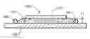
FIGS. 1 and 2 illustrate an exemplary die 110 that is attached to die pad 120 by conductive material 130 to form die attach package 100. As shown in FIG. 1, t1 is the BLT between the die 110 and the die attach pad 120. Increasing the BLT by increasing the thickness of the conductive material 130 decreases the shear stress on the die, which makes larger thicknesses more desirable. However, the low viscosity required to assure no voids usually limits the thickness to less than 3 mils. But increasing the amounts of conductive material used during die attach in effort to increase BLT can result in flow of the conductive material to other portions of the leadframe or the die, potentially causing moisture path, short circuits and problems in wire bonding and often resulting in failure of the semiconductor device.
To avoid these problems, some die attach processes use a “spanker” to flatten the conductive material during the die attach process. However, using the spanker involves extra steps that make the device fabrication process longer, less productive, and more expensive. Additionally, if too much conductive material is used to attempt to achieve a high BLT, the conductive material may be displaced by the spanker from the die attach pad to other portions of the leadframe, potentially causing short-circuits and other problems.
SUMMARY
This application describes die attach methods used in making semiconductor devices and the die packages and the semiconductor devices resulting from those methods. The methods include providing a leadframe with a die attach pad, using a boundary feature(s) containing a bond wire to define a perimeter on the die attach pad, depositing a conductive material (such as solder) within the perimeter, and then attaching a die containing an integrated circuit device to the die attach pad by using the conductive material. The boundary feature(s) allow an increased thickness of conductive material to be used, resulting in increased bond line thickness and increasing the durability and performance of the resulting semiconductor package.
BRIEF DESCRIPTION OF THE DRAWINGS
The following description can be better understood in light of Figures, in which:
FIG. 1 illustrates a perspective view of a known die package with a die bonded to a die attach pad of a leadframe;
FIG. 2 illustrates another view of the die package shown in FIG. 1;
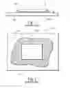
FIG. 3 illustrates a top view of an exemplary die package with boundary features containing a bond wire;
FIG. 4 illustrates a cross-sectional view of the die package shown in FIG. 3; and
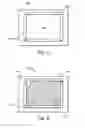
FIG. 5 shows a top view of some embodiments of a die attach pad containing boundary features formed on an upper surface thereof;
FIG. 6 illustrates a top view of some embodiments of a die attach pad with a conductive material formed between the boundary features;
FIGS. 7a and 7b shows perspective views of some embodiments of a die attached to the die attach pad with different configurations of bond wire connection points of the boundary feature; and
FIGS. 8a and 8b depict details of the bonds used to attach the bond wire of the boundary feature to the die attach pad.
The Figures illustrate specific aspects of the semiconductor devices and associated methods of making and using such devices. Together with the following description, the Figures demonstrate and explain the principles of the semiconductor devices and associated methods. In the drawings, the thickness of layers and regions are exaggerated for clarity. It will also be understood that when a layer is referred to as being “on” another layer or substrate, it can be directly on the other layer or substrate, or intervening layers may also be present. The same reference numerals in different drawings represent the same element, and thus their descriptions will not be repeated.
DETAILED DESCRIPTION
The following description supplies specific details in order to provide a thorough understanding. Nevertheless, the skilled artisan would understand that the apparatus and associated methods of using the apparatus can be implemented and used without employing these specific details. Indeed, the devices and associated methods can be placed into practice by modifying the illustrated devices and associated methods and can be used in conjunction with any other apparatus and techniques conventionally used in the industry. For example, while the description below focuses on die attach processes for semiconductor devices and packages, the devices and associated processes could be equally applied to any process or device where a die is connected to a die attach pad, such as a printed circuit board, MEMS devices, and the like.
One exemplary die package formed using the methods describe herein is illustrated in FIGS. 3 and 4. In FIG. 3, the die package 200 contains a die 210 bonded to a die attach pad 220 by conductive material 230. Boundary features 240 containing a bond wire form a perimeter on die attach pad 220 around the die 210 and the conductive material 230. As shown in FIG. 4, the conductive material 230 may be located between die 210 and die attach pad 220 with a bond line thickness (BLT) represented by a thickness t2.
The die 210 may comprise any type of semiconductor die known in the art. In some embodiments, the die comprises a silicon-based substrate containing any integrated circuit device known in the art. But in other embodiments, the die may also be made of GaAs, SiC, GaN, or any other suitable semiconductor material. The substrate and the integrated circuit device may have any configuration desired and needed to perform any desired function. For example, the die 210 may include one or more discrete transistors, diodes, or other known integrated circuit device. Thus, the die 210 may be designed to perform any number of functions, such as power regulation, memory, processing, or any other integrated circuit (IC) function. The die 210 may have any size needed for these functions. In some embodiments, the size of the die can range, for example, from about 100 μm by about 100 μm to about 20000 μm by about 20000 μm.
The die attach pad 220 may be a portion of any leadframe known in the art or may be a separate paddle. As well, the die attach pad 220 may be a single die attach pad of a leadframe, may be one of a plurality of die attach pads on a leadframe, or plurality of connected leadframes used in semiconductor manufacturing. When a leadframe is used, it is formed so that it is relatively planar in the area of the die attach pad 220. The leadframe serves as part of the I/O interconnection system, and also provides a thermally conductive path for dissipating the majority of the heat generated by the integrated circuit device in the die 210.
The material of the leadframe may comprise any metal, such as copper or a copper alloy. In some instances, the leadframe can contain a layer of metal plating (not shown), if desired. The layer of metal plating may comprise an adhesion sublayer, a conductive sublayer, and/or an oxidation resistant layer. For example, the leadframe may include a leadframe plating containing an adhesion sublayer and a wettable/protective sublayer.
The die 210 and the die attach pad 220 can be attached to each other by a conductive material (that forms a layer) 230. The conductive material 230 may be any conductive material that can attach these two components to each other. In some embodiments, the conductive material 230 comprises a solder that is configured to be used in a die attach process. For example, the conductive material 230 may be a Pb—Sn, Au—Sn, or other solder. Other solders that may be used as conductive material 230 may be made of Sn, Ag, and/or Pb—Sn—Ag. In some embodiments, the conductive material 230 may be an adhesive configured to be used in a die attach process. For example, an adhesive conductive material 230 may be a non-conductive or a conductive epoxy material like silver epoxy.
As shown in FIG. 4, the die package 200 contains wire-shaped boundary features 240 that form a perimeter on the die attach pad 220 around the area containing the conductive material 230. The boundary features 240 function to allow an increased amount of conductive material 230 to be used in the die bonding process, resulting in a higher BLT. In other words, the boundary features 240 comprise a raised surface of a sufficient height to make it a boundary for the conductive material 230.
FIG. 4 illustrates one example of the BLT that can be obtained and is represented by t2.
In some embodiments, t2 may range up to 30 mils. In other embodiments, this thickness can range from about 4 to about 30 mils.
The size of the perimeter defined by boundary features 240 depends on the size of the die and, therefore, the type of semiconductor device being made. In some embodiments, the perimeter can measure from about 100 μm by about 100 μm to about 20000 μm by about 20000 μm. And while the perimeter is illustrated as being substantially rectangular in shape, the shape will also depend on the shape of the die 210 and can therefore be substantially square, circular, triangular, or polygonal.
The boundary features 240 may form a complete or partial boundary. In some embodiments, and as shown in FIGS. 3 and 4, the wire bond of the boundary features may be applied to form a complete perimeter on the die attach pad 220. In other embodiments, the boundary features 240 may be applied to form a partial perimeter, such that about 75% or even 50% or more of the perimeter is defined by the wire bond of the boundary features 240.
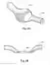
In some embodiments, the boundary features 240 may comprise 1 or more bond wires that can be bonded to the die attach pad 220. In some configurations, and as shown in FIG. 7b, 4 bond wires (such as those wires that are known to be used to attach a die to a lead finger), can be bonded to the die attach pad 220 so as to form the perimeter that will contain the conductive material 230. In other configurations as illustrated in FIG. 7a, a single segment of a bond wire can be bonded at various points of the wire to form the perimeter. Additionally, any number of segments of wire may be bonded to form the wire as is convenient or necessary to form the perimeter.
Each bond wire can be attached to the die attach pad 220 using any technique known in the art. In some embodiments, the bond wire(s) can be attached to the die attach pad 220 by using a stitch and/or wedge bond 250 at each end, as shown in FIGS. 8a and 8b. Where longer bond wires are used, one or more stitch and/or wedge bonds between the ends of the bond wires can be included as needed.
These structures described above may be formed using any known process that will form the structures illustrated above. In some embodiments, the die 210 can be manufactured by providing the various electronic components (i.e., the transistors) in a semiconductor substrate as known in the art. In other embodiments, the integrated circuits are manufactured, cut, tested, and die-bonded to a substrate as known in the art.
Next, a leadframe can be formed by any known method, for example, by any metal stamping and etching processes. If desired, a layer of metal plating may be formed on the base metal used in the leadframe by processes such as electroless plating, sputtering, or electroplating. A pre-plated leadframe can also be used instead. The leadframe is made with the die pad 220 formed as part of the leadframe.
Next, the bond wire can be attached to the die attach pad 220 using any known technique. In some embodiments, the boundary features 240 may be attached using a bond wire stitching technique known in the art. The bond wire of the boundary features 240 may be connected (i.e., by using a stitch or wedge bond 250 as illustrated in FIGS. 8a and 8b) to the die attach pad 220 using any number of connection points. In one example, and as shown in FIG. 7b, the boundary feature is connected along the perimeter using a stitch and/or wedge bond 250 having multiple attach points along the perimeter. In another example as shown in FIG. 7a, any side of the perimeter may have as many connection points as needed, including from 4 to 40 stitch and/or wedge bonds.
FIGS. 8a and 8b show a detailed view of a bond wire stitch that can be used to connect the bond wire of the boundary feature to the die attach pad. As known in the art of wedge/stitch wire bonding, the wire becomes deformed at the point of attachment to the die attach pad, as illustrated in FIG. 8a. FIG. 8b shows a cross sectional view of the bond wire and its stitch bond attachment. The wedge/stitch bond used with the boundary features 240 may be used at any point(s) along the perimeter to provide the needed connection for the bond wire.
Next in the manufacturing process, as shown in FIG. 6, the conductive material 230 can be deposited onto the die attach pad 220 within the perimeter defined by the boundary features 240. The conductive material can be deposited using any known process until the desired height is reached that will provide the desired BLT. In some embodiments, a spanker may be used to flatten the conductive material 230. In other embodiments, though, no spanker is used due to the possibility of conductive material 230 being displaced or splashed out of the perimeter defined by the boundary features 240.
Then, the die 210 is then placed onto the conductive material 230 using any known process in the art. The resulting structure can then be heated at a sufficient time and temperature that will re-flow the conductive material 230 without changing the shape of the bond wire used in the boundary feature(s) 240. During the re-flow process, the conductive material 230 is forced to stay with the perimeter established by the boundary feature 240. After the reflow process is complete, the die 210 is attached to the die attach pad 220 by the reflowed conductive material 230 that has the desired height, yet has substantially no voids.
Once the die package has been formed in this manner, further processing can be performed to make a semiconductor device. For example, electrical connections may be established between portions of integrated circuit device on the die and portions of the lead fingers using wires, usually with a wire bonding process. After the wire bonding process, a resin body can be formed to encapsulate the die and the wirebonds. The resulting structure may then be singulated (and optionally tested) to create a semiconductor package with leads. The package leads can then be connected to another electrical device, such as a printed circuit board (or PCB) so that it is connected electrically to the integrated circuit of the die.
The die packages described above have several advantages. First, a higher BLT allows for more robust die packages, limiting the mechanical failure of die 210 due to cracking and due to voids in conductive material 230. The higher BLT also can result in increased thermal performance, limiting the failure rate of die 210.
In addition to any previously indicated modification, numerous other variations and alternative arrangements may be devised by those skilled in the art without departing from the spirit and scope of this description, and appended claims are intended to cover such modifications and arrangements. Thus, while the information has been described above with particularity and detail in connection with what is presently deemed to be the most practical and preferred aspects, it will be apparent to those of ordinary skill in the art that numerous modifications, including, but not limited to, form, function, manner of operation and use may be made without departing from the principles and concepts set forth herein. Also, as used herein, examples are meant to be illustrative only and should not be construed to be limiting in any manner.
Claims
1. A die package for a semiconductor device, the die package comprising:
a leadframe containing a die attach pad;
a conductive layer on a portion of the die attach pad, wherein the conductive layer has a thickness ranging up to about 30 mil;
a boundary feature comprising a bond wire partially surrounding the conductive layer, wherein both ends of the bond wires are attached to the die attach pad; and
a die on the conductive layer.
2. The die package of claim 1, wherein the boundary feature completely surrounds the conductive layer.
3. The die package of claim 1, wherein the boundary feature surrounds at least half of the conductive layer.
4. The die package of claim 1, wherein the conductive layer has a thickness ranging from about 4 mil to about 30 mil.
5. The die package of claim 1, wherein the conductive layer is substantially free of voids between the die and the die attach pad.
6. The die package of claim 1, wherein both ends of the bond wire have been attached to the die attach pad using a wedge or stitch bond.
7. The die package of claim 6, wherein the bond wire has been attached to the die attach pad at more than two locations.
8. The die package of claim 1, wherein four bond wires are used to make the boundary feature and both ends of each bond wire are attached to the die attach pad.
9. A semiconductor device, the comprising:
a leadframe containing a die attach pad;
a conductive layer on a portion of the die attach pad, wherein the conductive layer has a thickness ranging up to about 30 mil;
a boundary feature comprising a bond wire partially surrounding the conductive layer, wherein both ends of the bond wires are attached to the die attach pad; and
a die on the conductive layer.
10. The device of claim 9, wherein the boundary feature completely surrounds the conductive layer.
11. The device of claim 9, wherein the boundary feature surrounds at least half of the conductive layer.
12. The device of claim 9, wherein the conductive layer has a thickness ranging from about 4 mil to about 30 mil.
13. The device of claim 9, wherein the conductive layer is substantially free of voids between the die and the die attach pad.
14. The device of claim 9, wherein both ends of the bond wire have been attached to the die attach pad using a wedge or stitch bond.
15. The device of claim 14, wherein the bond wire has been attached to the die attach pad at more than two locations.
16. The device of claim 9, wherein four bond wires are used to make the boundary feature and both ends of each bond wire are attached to the die attach pad.
17. A method for making a semiconductor device, comprising:
providing a leadframe containing a die attach pad;
forming a boundary feature comprising a bond wire so that both ends of the bond wire are attached to the die attach pad, the boundary feature defining a periphery;
depositing a conductive layer on the die attach pad within the periphery, wherein the conductive layer has a thickness ranging up to about 30 mil;
placing a die on the conductive layer; and
reflowing the conductive layer to attach the die to the die attach pad.
18. The method of claim 17, wherein the reflowed conductive layer is substantially free of voids between the die and the die attach pad.
19. The method of claim 17, wherein the conductive layer comprises a solder based material.
20. The method of claim 17, wherein the periphery of the boundary feature surrounds at least half of the conductive layer.
21. The method of claim 20, wherein the periphery of the boundary feature completely surrounds the conductive layer.
22. The method of claim 17, wherein both ends of the bond wire have been attached to the die attach pad using a wedge or stitch bond.
23. The method of claim 17, further comprising attaching the bond wire to the die attach pad at more than two locations.
24. The method of claim 17, wherein four bond wires are used to make the boundary feature and both ends of each bond wire are attached to the die attach pad.
25. The method of claim 17, wherein the conductive layer has a thickness ranging from about 4 mil to about 30 mil.
Images & Drawings included:


Sources:
- United States Patent and Trademark Office - verify current appl. status at the USPTO↗
Similar patent applications:
- » 20090115039
High bond line thickness for semiconductor devices
Recent applications in this class:
- » 20250286009 2025-09-11
JOINING STRUCTURE AND JOINING MATERIAL FOR FORMING JOINING PART OF SAID JOINING STRUCTURE - » 20250286008 2025-09-11
SEMICONDUCTOR DEVICE AND SEMICONDUCTOR MODULE - » 20250279387 2025-09-04
Display Device - » 20250259960 2025-08-14
ELECTRONIC MODULE - » 20250259959 2025-08-14
SEMICONDUCTOR PACKAGE AND METHOD OF FABRICATING THE SAME - » 20250253282 2025-08-07
STORAGE LAYERS FOR WAFER BONDING - » 20250253281 2025-08-07
Through-substrate laser soldering with embedded absorbing layer - » 20250239558 2025-07-24
SUBSTRATE STRUCTURE AND MANUFACTURING METHOD THEREOF - » 20250226350 2025-07-10
PACKAGING STRUCTURE OF RF FRONT-END MODULE - » 20250226349 2025-07-10
SEMICONDUCTOR PACKAGE AND METHOD OF MANUFACTURING THE SAME
Recent applications for this Assignee:
- » 20170025847 2017-01-26
Ground fault circuit interrupter (GFCI) monitor - » 20170005583 2017-01-05
Control of a startup circuit using a feedback pin of a PWM controller integrated circuit chip - » 20160285368 2016-09-29
Artificial ripple modulation control circuitry - » 20160284871 2016-09-29
Avalanche-rugged silicon carbide (SiC) power Schottky rectifier - » 20160261201 2016-09-08
Power supply with near valley switching - » 20160261196 2016-09-08
Power supply with line compensation circuit - » 20160241016 2016-08-18
Adaptive overvoltage protection for adaptive power adapters - » 20160222939 2016-08-04
Ignition control circuit with current slope detection - » 20160190308 2016-06-30
Silicon-carbide trench gate MOSFETs - » 20160190300 2016-06-30
Silicon carbide (SiC) device with improved gate dielectric shielding