Circuit Device
US20120025898A1
2012-02-02
12/900,221
2010-10-07
Abstract:
A circuit device includes an option pad, a first power source pad, and a first ground pad, wherein the option pad, the first power source pad, and the first ground pad are formed over various portions of a top surface of the circuit device, and a function of the circuit device is determined by coupling the option pad with one of the first power source pad and the first ground pad through a wire bond.
Assignee:
- RICHWAVE TECHNOLOGY CORP. 225 🇹🇼 Taipei, Taiwan
Interested in similar patents?
Get notified when new applications in this technology area are published.
Classification:
H01L24/49 » CPC main
Arrangements for connecting or disconnecting semiconductor or solid-state bodies; Methods or apparatus related thereto; Means for bonding being attached to, or being formed on, the surface to be connected, e.g. chip-to-package, die-attach, "first-level" interconnects; Manufacturing methods related thereto; Wire connectors; Manufacturing methods related thereto; Structure, shape, material or disposition of the wire connectors after the connecting process of a plurality of wire connectors
H01L23/50 » CPC further
Details of semiconductor or other solid state devices; Arrangements for conducting electric current to or from the solid state body in operation, e.g. leads, terminal arrangements ; Selection of materials therefor for integrated circuit devices, e.g. power bus, number of leads
H01L24/06 » CPC further
Arrangements for connecting or disconnecting semiconductor or solid-state bodies; Methods or apparatus related thereto; Means for bonding being attached to, or being formed on, the surface to be connected, e.g. chip-to-package, die-attach, "first-level" interconnects; Manufacturing methods related thereto; Bonding areas ; Manufacturing methods related thereto; Structure, shape, material or disposition of the bonding areas prior to the connecting process of a plurality of bonding areas
H01L24/48 » CPC further
Arrangements for connecting or disconnecting semiconductor or solid-state bodies; Methods or apparatus related thereto; Means for bonding being attached to, or being formed on, the surface to be connected, e.g. chip-to-package, die-attach, "first-level" interconnects; Manufacturing methods related thereto; Wire connectors; Manufacturing methods related thereto; Structure, shape, material or disposition of the wire connectors after the connecting process of an individual wire connector
H01L2224/0612 » CPC further
Indexing scheme for arrangements for connecting or disconnecting semiconductor or solid-state bodies and methods related thereto as covered by; Means for bonding being attached to, or being formed on, the surface to be connected, e.g. chip-to-package, die-attach, "first-level" interconnects; Manufacturing methods related thereto; Bonding areas; Manufacturing methods related thereto; Structure, shape, material or disposition of the bonding areas prior to the connecting process of a plurality of bonding areas; Disposition Layout
H01L2224/4813 » CPC further
Indexing scheme for arrangements for connecting or disconnecting semiconductor or solid-state bodies and methods related thereto as covered by; Means for bonding being attached to, or being formed on, the surface to be connected, e.g. chip-to-package, die-attach, "first-level" interconnects; Manufacturing methods related thereto; Wire connectors; Manufacturing methods related thereto; Structure, shape, material or disposition of the wire connectors after the connecting process of an individual wire connector; Disposition Connecting within a semiconductor or solid-state body, i.e. fly wire, bridge wire
H01L2924/01033 » CPC further
Indexing scheme for arrangements or methods for connecting or disconnecting semiconductor or solid-state bodies as covered by; Chemical elements Arsenic [As]
H01L2924/10253 » CPC further
Indexing scheme for arrangements or methods for connecting or disconnecting semiconductor or solid-state bodies as covered by; Details of semiconductor or other solid state devices to be connected; Material of the semiconductor or solid state bodies; Semiconducting materials; Elemental semiconductors, i.e. Group IV Silicon [Si]
H01L2224/45099 » CPC further
Indexing scheme for arrangements for connecting or disconnecting semiconductor or solid-state bodies and methods related thereto as covered by; Means for bonding being attached to, or being formed on, the surface to be connected, e.g. chip-to-package, die-attach, "first-level" interconnects; Manufacturing methods related thereto; Wire connectors; Manufacturing methods related thereto; Structure, shape, material or disposition of the wire connectors prior to the connecting process of an individual wire connector; Core members of the connector Material
H01L2924/00014 » CPC further
Indexing scheme for arrangements or methods for connecting or disconnecting semiconductor or solid-state bodies as covered by; Technical content checked by a classifier the subject-matter covered by the group, the symbol of which is combined with the symbol of this group, being disclosed without further technical details
H01L2224/05599 » CPC further
Indexing scheme for arrangements for connecting or disconnecting semiconductor or solid-state bodies and methods related thereto as covered by; Means for bonding being attached to, or being formed on, the surface to be connected, e.g. chip-to-package, die-attach, "first-level" interconnects; Manufacturing methods related thereto; Bonding areas; Manufacturing methods related thereto; Structure, shape, material or disposition of the bonding areas prior to the connecting process of an individual bonding area; External layer Material
H01L2924/14 » CPC further
Indexing scheme for arrangements or methods for connecting or disconnecting semiconductor or solid-state bodies as covered by; Details of semiconductor or other solid state devices to be connected; Device type Integrated circuits
H01L2924/00 » CPC further
Indexing scheme for arrangements or methods for connecting or disconnecting semiconductor or solid-state bodies as covered by
H03K17/00 IPC
Electronic switching or gating, i.e. not by contact-making and –breaking
Description
CROSS REFERENCE TO RELATED APPLICATIONS
This Application claims priority of Taiwan Patent Application No. 99125307, filed on Jul. 30, 2010, the entirety of which is incorporated by reference herein.
BACKGROUND OF THE INVENTION
1. Field of the Invention
The present invention relates to integrated circuit fabrication, and in particular relates to a circuit device with bonding-option structures.
2. Description of the Related Art
In the design of an integrated circuit (IC), a bonding option structure is usually provided for the IC so as to selectively alter an aspect of the hardware configuration in the IC. Thus, various aspects of hardware configuration in a circuit chip of an integrated circuit such as internal logic functions, specific functions, and clocking functions thereof can be selectively altered by manufacturers according to various application needs; thereby providing integrated circuit devices with similar hardware structures having multiple options.
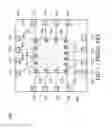
One of the conventional bonding option structures is a power/ground bonding option structure. In FIG. 1, a conventional integrated circuit (IC) device 300 using a power/ground bonding option structure is illustrated.
As shown in FIG. 1, a top view of the IC device 300 is illustrated. The IC device 300 comprises a package substrate 100 and a circuit device 200 disposed over a portion of the package substrate 100. Herein, the circuit device 200 can be disposed over the package substrate 100 by packaging techniques such as a surface mounting technology (SMT).
In one embodiment, the circuit device 200 can be a semiconductor chip fabricated from a silicon wafer, and a plurality of bonding pads 202, 204, 206, 208, 210, 212, 214, 216, 218, 220, 222, 224, 226, 228, and 230 are separately disposed over various portions of a top surface of the circuit device 200 around an edge thereof. In one embodiment, the package substrate 100 can be formed of, for example, ceramic substrates or printed circuit boards (PCBs), and a plurality of bonding elements 1021, 1022, 1041, 1042, 106, 108, 110, 112, 114, 116, 118, 120, 122, 124, 126, and 128 can be disposed on various portions over a top surface of the package substrate 100 around an edge thereof.
In FIG. 1, the bonding elements 1021, 1022, 1041, 1042, 106, 108, 110, 112, 114, 116, 118, 120, 122, 124, 126, and 128 are illustrated as conductive bonding pads, but are not limited thereto, and the bonding elements can be also provided as other configurations such as leads or pins.
Still referring to FIG. 1, the bonding elements 106, 108, 110, 112, 114, 116, 118, 120, 122, 124, 126, and 128 disposed over the packaging substrate 100 may be used for functional circuit elements such as input/output, control, or clocking elements, and the bonding elements 1021 and 1022 may be used as power source elements, and the bonding elements 1041, 1042 may be used as ground elements. The bonding pads 202 and 204 formed over the top surface of the circuit device 200 may function as a power source pad and a ground pad, respectively, and are electrically connected to the bonding element 1021 as a power source element and the bonding element 1041 as a ground element. The bonding pad 206 may function as an option pad and is coupled to the bonding structure 1022 which also functions as a power source element by a wire 400 or is coupled to the bonding structure 1042 which also functions as a ground element by a wire 400′ (illustrated in dotted lines); thereby allowing related circuit functions such as internal logic functions, specific functions, or clocking functions in the circuit device 200 of the IC device 300 to be assigned. The other bonding pads 208, 210, 212, 214, 216, 218, 220, 222, 224, 226, 228, and 230 disposed over the top surface of the circuit device 200 may provided for other functional circuit pads such as input/output, control, and clocking pads and can be respectively coupled to one of the bonding elements 106, 108, 110, 112, 114, 116, 118, 120, 122, 124, 126, and 128 disposed over the packaging substrate 100 by wire bond methods; thereby providing electrical connections between the circuit device 200 and the packaging substrate 100.
As shown in FIG. 1, although the two possible coupling configurations between the option pad 206 and the bonding element 1021 functioning as a power source element or the bonding element 1041 functioning as a ground element can be used for assigning related circuit functions such as internal logic functions, specific functions, and clocking functions of the circuit device 200 such that the IC device 300 is provided with two different functions. The bonding elements 1022 and 1042, however, are additional power source and ground bonding elements formed over the packaging substrate 100; thereby requiring increased surface area of the packaging substrate 100 since the bonding elements are additionally formed over the packaging substrate 100. In addition, formations of the bonding elements 1022 and 1042 may occupy areas where other functional circuit elements may be formed; thereby decreasing amounts of bonding elements for electrically connecting the functional circuit bonding pads formed over the circuit device 200.
The above power/ground bonding elements used in the IC device 300 are unfavorable for size reduction of the package substrate 100 therein and positions of the bonding elements formed thereon may be thus occupied.
BRIEF SUMMARY OF THE INVENTION
Therefore, an improved power/ground bonding option structure is needed for mitigating the above problems found in the conventional power/ground bonding option structures.
Circuit devices with improved circuit/ground bonding option pads capable of mitigating the above mentioned problems are provided.
An exemplary circuit device comprises an option pad, a first power source pad, and a first ground pad, wherein the option pad, the first power source pad, and the first ground pad are formed over various portions of a top surface of the circuit device, and a function of the circuit device is determined by coupling the option pad with one of the first power source pad and the first ground pad through a wire bond.
A detailed description is given in the following embodiments with reference to the accompanying drawings.
BRIEF DESCRIPTION OF THE DRAWINGS
The present invention can be more fully understood by reading the subsequent detailed description and examples with references made to the accompanying drawings, wherein:
FIG. 1 is a schematic diagram showing a conventional integrated circuit device having a bonding option structure;
FIG. 2 is a schematic diagram showing an integrated circuit device having a bonding option structure according to an embodiment of the invention; and
FIG. 3 is a schematic diagram showing an integrated circuit device having a bonding option structure according to another embodiment of the invention.
DETAILED DESCRIPTION OF THE INVENTION
The following description is of the best-contemplated mode of carrying out the invention. This description is made for the purpose of illustrating the general principles of the invention and should not be taken in a limiting sense. The scope of the invention is best determined by reference to the appended claims.
FIGS. 2-3 are schematic diagrams showing exemplary embodiments of the invention. In the figures, the same references represent the same elements.
In FIG. 2, an integrated circuit (IC) device 500 using a power/ground bonding option structure according to an embodiment of the invention is illustrated.
As shown in FIG. 2, a top view of the IC device 500 is illustrated. The IC device 500 comprises a package substrate 600 and a circuit device 700 disposed over a portion of the package substrate 600. Herein, the circuit device 700 can be disposed over the package substrate 600 by packaging techniques such as a surface mounting technology (SMT) packaging technique.
In one embodiment, the circuit device 700 can be a semiconductor chip fabricated from a silicon wafer, and a plurality of bonding pads 7021, 7022, 7061, 7062, 710, 712, 714, 716, 718, 720, 722, 724, 726, 728, 730, 732, and 734 are separately disposed over various portions of a top surface of the circuit device 700 around an edge thereof. In one embodiment, the package substrate 600 can be formed of, for example, ceramic substrates or printed circuit boards (PCBs), and a plurality of bonding elements 602, 604, 606, 608, 610, 612, 614, 616, 618, 620, 622, 624, 626, 628, 630, and 632 can be disposed on various portions over a top surface of the package substrate 600 around an edge thereof.
In FIG. 2, the bonding elements 602, 604, 606, 608, 610, 612, 614, 616, 618, 620, 622, 624, 626, 628, 630, and 632 are illustrated as conductive bonding pads, but are not limited thereto, and the bonding elements can be also provided as other configurations such as leads or pins.
Still referring to FIG. 2, the bonding elements 602, 604, 606, 608, 610, 612, 614, 616, 618, 620, 622, 624, 626, 628, 630, and 632 disposed over the packaging substrate 600 may be used as functional circuit elements such as input/output, control, or clocking elements, and the bonding element 602 may be used as a power source element, and the bonding elements 604 may be used as a ground element. The bonding pads 7021 and 7022 formed over various portions of the top surface of the circuit device 700 may function as power source pads, and the bonding pads 7021 and 7022 are electrically connected by a power source bus line 704 (illustrated as dotted lines) disposed in the circuit device 700. The bonding pads 7061 and 7062 formed over various portions of the top surface of the circuit device 700 may function as ground pads, and the bonding pads 7061 and 7062 are electrically connected by a ground bus line 708 (illustrated as dotted lines) disposed in the circuit device 700. One of the bonding pads 7021 and 7022 and one of the bonding pads 7061 and 7062 are coupled to the bonding element 602 as a power source element and the bonding element 604 as a ground element, respectively. The bonding pad 710 disposed over the circuit device 700 may function as an option pad and is coupled to one of the bonding pads 7021 and 7022 which function as a power source bonding pads by a wire 800 or one of the bonding pads 7061 and 7062 which function as a ground bonding pad by a wire 800′ (illustrated in dotted lines); thereby allowing related circuit functions such as internal logic functions, specific functions, or clocking functions in the circuit device 700 of the IC device 500 to be assigned. It is noted that the wire 800 coupled to the power source element or the ground element over the package substrate is not formed over the power source pad or the ground pad coupled to the bonding pad 710 which functions as the bonding option pad. The other bonding pads 712, 714, 716, 718, 720, 722, 724, 726, 728, 730, 732 and 734 disposed over the top surface of the circuit device 700 may provide for other functional circuit pads such as input/output, control, and clocking pads and can be respectively coupled to one of the bonding elements 610, 612, 614, 616, 618, 620, 622, 624, 626, 628, 630 and 632 disposed over the packaging substrate 600 by wire bonds; thereby providing electrical connections between the circuit device 700 and the packaging substrate 600.
As shown in FIG. 2, though the electrically connected two power source pads (e.g. the bonding pads 7021 and 7022) and the two ground pads (e.g. the bond pads 7061 and 7062), and through the two possible coupling configurations between the bonding option pad 710 and one of the bonding pads 7021 and 7022 functioning as a power source pad and one of the bonding pad 7061 and 7062 functioning as a ground pad, related circuit functions such as internal logic functions, specific functions, and clocking functions of the circuit device 700 can be assigned such that the IC device 500 is provided with two different functions. Thus, there is no need to additionally provide the bonding elements 1022 and 1042 functioning as power source and ground elements of the integrated circuit device 300 shown in FIG. 1 over the package substrate 600, saving usable areas over the package substrate 600 and increasing the bonding pads for functional circuit pads over the package substrate 600 for adequately utilizing surface areas over the package substrate 600. In addition, through the connections of the bonding pad 710, functioning as ? option pads as shown in FIG. 2, amounts of the bonding pads 712, 714, 716, 718, 720, 722, 724, 726, 728, 730, 732 and 734 can be decreased according size reduction demand of the circuit device 700, and amounts of the bonding elements 610, 612, 614, 616, 618, 620, 622, 624, 626, 628, 630 and 632 over the package substrate 600 can be correspondingly decreased such that size of the IC device 500 is reduced. Thus, usage of the power/ground bonding option structure of the IC device 500 shown in FIG. 2 is advantageous for size reduction of the circuit device 700 and the package substrate 600.
In FIG. 2, the option pad 710 is illustrated as being adjacent to a side of the bonding pad 7062 functioning as a ground pad but is not limited thereto. In another embodiment, the option pad 710 can be also disposed at different locations such as at a place between the bonding pads 720 and 722, as shown in FIG. 3.
In the exemplary embodiments shown in FIGS. 2 and 3, the bonding pads 7021 and 7022 are not limited to being power source pads and may function as ground pads while the bonding element 602 over the package substrate 600 functions as a ground element. Similarly, in the exemplary embodiments shown in FIGS. 2 and 3, the bonding pads 70261 and 7062 are not limited to functioning as ground pads and may function as power source pads while the bonding element 604 over the package substrate 600 functions as a power source element. Functions of the above elements can be properly adjusted according to practical applications.
While the invention has been described by way of example and in terms of the preferred embodiments, it is to be understood that the invention is not limited to the disclosed embodiments. To the contrary, it is intended to cover various modifications and similar arrangements (as would be apparent to those skilled in the art). Therefore, the scope of the appended claims should be accorded the broadest interpretation so as to encompass all such modifications and similar arrangements.
Claims
What is claimed is:1. A circuit device, comprising
an option pad;
a first power source pad; and
a first ground pad, wherein the option pad, the first power source pad, and the first ground pad are formed over various portions of a top surface of the circuit device, and a function of the circuit device is determined by coupling the option pad with one of the first power source pad and the first ground pad through a wire bond.
2. The circuit device as claimed in claim 1, further comprising a plurality of functional circuit pads separately disposed over various portions of the top surface of the circuit device, wherein the functional circuit pads are formed over various portions of the circuit device around an edge thereof, and the function circuit pads are formed at locations different from that of the option pad, the first power source pad, and the first ground pad.
3. The circuit device as claimed in claim 1, further comprising a second power source pad formed over a portion of the top surface of the circuit device and adjacent to the first power source pad.
4. The circuit device as claimed in claim 3, further comprising a first power bus line disposed in the circuit device to electrically connect the first power source pad to the second power source pad.
5. The circuit device as claimed in claim 1, further comprising a second ground pad disposed over a portion of the top surface of the circuit device and adjacent to the first ground pad.
6. The circuit device as claimed in claim 1, further comprising a first ground bus line disposed in the circuit device to electrically connect the first ground pad to the second ground pad.
Images & Drawings included:


Sources:
- United States Patent and Trademark Office - verify current appl. status at the USPTO↗
Similar patent applications:
- » 20130322888
OPTICAL TRANSMISSION CIRCUIT DEVICE, OPTICAL RECEPTION CIRCUIT DEVICE, OPTICAL TRANSMISSION/RECEPTION CIRCUIT DEVICE AND OPTICAL TRANSMISSION METHOD - » 20070285149
Switch circuit device, and wireless circuit device and sampling circuit device employing the same - » 20080028349
Method for identifying semiconductor integrated circuit device, method for manufacturing semiconductor integrated circuit device, semiconductor integrated circuit device and semiconductor chip - » 20090249264
Analyzing device for circuit device, circuit device analyzing method, analyzing program, and electronic medium - » 20050263605
Method for identifying semiconductor integrated circuit device, method for manufacturing semiconductor integrated circuit device, semiconductor integrated circuit device and semiconductor chip - » 20050175984
Molecular device, molecule array, rectifier device, rectifying method, sensor device, switching device, circuit device, logical circuit device, operational device and information processing device - » 20240372444
METHOD FOR PRODUCING AN ELECTRICAL CIRCUIT DEVICE FOR OPERATING AN EXTERNALLY EXCITED ELECTRIC MACHINE, ELECTRICAL CIRCUIT DEVICE FOR OPERATING AN EXTERNALLY EXCITED ELECTRIC MACHINE, ELECTRIC DRIVE DEVICE COMPRISING AN ELECTRICAL CIRCUIT DEVICE, AND MOTOR VEHICLE COMPRISING AN ELECTRIC DRIVE DEVICE - » 20090033300
Output control device, and AC/DC power source device, circuit device, LED backlight circuit device, and switching DC/DC converter device each using output control device - » 20100038799
Semiconductor integrated circuit device, mounting structure of semiconductor integrated circuit device, and method for manufacturing semiconductor integrated circuit device - » 20050018461
Semiconductor integrated circuit device, method of testing semiconductor integrated circuit device and method of manufacturing semiconductor integrated circuit device
Recent applications in this class:
- » 20250054902 2025-02-13
Semiconductor Device and Method Using Lead Frame Interposer in Bump Continuity Test - » 20250022835 2025-01-16
SEMICONDUCTOR MODULE - » 20250006688 2025-01-02
OUTPUT MATCHING NETWORK TO REDUCE SELF AND MUTUAL INDUCTANCES OF OUTPUT INDUCTIVE COMPONENTS IN A CAVITY PACKAGE - » 20240347499 2024-10-17
SEMICONDUCTOR PACKAGE - » 20240312950 2024-09-19
SEMICONDUCTOR DEVICE - » 20240312949 2024-09-19
LAYOUT STRUCTURE OF DIFFERENTIAL LINES, MEMORY STORAGE DEVICE AND MEMORY CONTROL CIRCUIT UNIT - » 20240304591 2024-09-12
SEMICONDUCTOR DEVICE FOR AUDIO - » 20240203932 2024-06-20
POWER MODULE WITH IMPROVED ELECTRICAL COMPONENTS - » 20240145426 2024-05-02
BONDING STRUCTURE AND POWER DEVICE - » 20240145425 2024-05-02
Bond pad connection layout
Recent applications for this Assignee:
- » 20250172680 2025-05-29
TRANSCEIVING METHOD OF SIGNALS AND RADAR APPARATUS - » 20250172679 2025-05-29
TRANSCEIVING METHOD OF SIGNALS AND RADAR APPARATUS - » 20250169194 2025-05-22
ELECTROSTATIC DISCHARGE PROTECTION CIRCUIT - » 20250167742 2025-05-22
RADIO FREQUENCY POWER AMPLIFIER - » 20250167542 2025-05-22
TRANSISTOR STACK CIRCUIT - » 20250150147 2025-05-08
BEAM SWITCHING SYSTEM, BEAM SWITCHING METHOD, AND ANTENNA APPARATUS - » 20250150042 2025-05-08
BIAS CIRCUIT - » 20250118708 2025-04-10
FRONT-END CIRCUIT AND SEMI-CONDUCTOR DEVICE - » 20250105804 2025-03-27
AMPLIFY DEVICE AND SEMICONDUCTOR DEVICE - » 20250062756 2025-02-20
PROTECTION CIRCUIT AND PROTECTION METHOD