Semiconductor device and manufacturing method of a semiconductor device
US20120135568A1
2012-05-31
13/368,550
2012-02-08
✅ Patent granted
US 8,354,298 B2
2013-01-15
-
-
Roy Potter
2032-02-08
Abstract:
A semiconductor device of the present invention comprises a substrate and a first semiconductor element. The substrate comprises an inner layer conductor and a cavity comprising the bottom surface on which a part of the inner layer conductor is exposed. The first semiconductor element contacts, in the cavity, the inner layer conductor directly or via a good heat conductor material.
Assignee:
- NEC Corporation 20,055 🇯🇵 Tokyo, Japan
Applicant:
Interested in similar patents?
Get notified when new applications in this technology area are published.
Classification:
H01L21/50 IPC
Processes or apparatus adapted for the manufacture or treatment of semiconductor or solid state devices or of parts thereof; Manufacture or treatment of semiconductor devices or of parts thereof the devices having at least one potential-jump barrier or surface barrier, e.g. PN junction, depletion layer or carrier concentration layer Assembly of semiconductor devices using processes or apparatus not provided for in a single one of the subgroups - , e.g. sealing of a cap to a base of a container
H01L25/0657 » CPC main
Assemblies consisting of a plurality of individual semiconductor or other solid state devices ; Multistep manufacturing processes thereof all the devices being of a type provided for in the same subgroup of groups - , e.g. assemblies of rectifier diodes the devices not having separate containers the devices being of a type provided for in group Stacked arrangements of devices
H01L23/13 » CPC further
Details of semiconductor or other solid state devices; Mountings, e.g. non-detachable insulating substrates characterised by the shape
H01L23/49816 » CPC further
Details of semiconductor or other solid state devices; Arrangements for conducting electric current to or from the solid state body in operation, e.g. leads, terminal arrangements ; Selection of materials therefor consisting of soldered constructions; Leads, on insulating substrates,; Additional leads joined to the metallisation on the insulating substrate, e.g. pins, bumps, wires, flat leads Spherical bumps on the substrate for external connection, e.g. ball grid arrays [BGA]
H01L23/49822 » CPC further
Details of semiconductor or other solid state devices; Arrangements for conducting electric current to or from the solid state body in operation, e.g. leads, terminal arrangements ; Selection of materials therefor consisting of soldered constructions; Leads, on insulating substrates, Multilayer substrates
H01L24/73 » CPC further
Arrangements for connecting or disconnecting semiconductor or solid-state bodies; Methods or apparatus related thereto Means for bonding being of different types provided for in two or more of groups , , , , , , ,
H01L24/83 » CPC further
Arrangements for connecting or disconnecting semiconductor or solid-state bodies; Methods or apparatus related thereto; Methods for connecting semiconductor or other solid state bodies using means for bonding being attached to, or being formed on, the surface to be connected using a layer connector
H01L24/92 » CPC further
Arrangements for connecting or disconnecting semiconductor or solid-state bodies; Methods or apparatus related thereto; Methods for connecting semiconductor or solid state bodies including different methods provided for in two or more of groups - Specific sequence of method steps
H01L23/3677 » CPC further
Details of semiconductor or other solid state devices; Arrangements for cooling, heating, ventilating or temperature compensation ; Temperature sensing arrangements; Selection of materials, or shaping, to facilitate cooling or heating, e.g. heatsinks; Cooling facilitated by shape of device Wire-like or pin-like cooling fins or heat sinks
H01L24/16 » CPC further
Arrangements for connecting or disconnecting semiconductor or solid-state bodies; Methods or apparatus related thereto; Means for bonding being attached to, or being formed on, the surface to be connected, e.g. chip-to-package, die-attach, "first-level" interconnects; Manufacturing methods related thereto; Bump connectors ; Manufacturing methods related thereto; Structure, shape, material or disposition of the bump connectors after the connecting process of an individual bump connector
H01L24/32 » CPC further
Arrangements for connecting or disconnecting semiconductor or solid-state bodies; Methods or apparatus related thereto; Means for bonding being attached to, or being formed on, the surface to be connected, e.g. chip-to-package, die-attach, "first-level" interconnects; Manufacturing methods related thereto; Layer connectors, e.g. plate connectors, solder or adhesive layers; Manufacturing methods related thereto; Structure, shape, material or disposition of the layer connectors after the connecting process of an individual layer connector
H01L24/48 » CPC further
Arrangements for connecting or disconnecting semiconductor or solid-state bodies; Methods or apparatus related thereto; Means for bonding being attached to, or being formed on, the surface to be connected, e.g. chip-to-package, die-attach, "first-level" interconnects; Manufacturing methods related thereto; Wire connectors; Manufacturing methods related thereto; Structure, shape, material or disposition of the wire connectors after the connecting process of an individual wire connector
H01L2224/04042 » CPC further
Indexing scheme for arrangements for connecting or disconnecting semiconductor or solid-state bodies and methods related thereto as covered by; Means for bonding being attached to, or being formed on, the surface to be connected, e.g. chip-to-package, die-attach, "first-level" interconnects; Manufacturing methods related thereto; Bonding areas; Manufacturing methods related thereto; Structure, shape, material or disposition of the bonding areas prior to the connecting process Bonding areas specifically adapted for wire connectors, e.g. wirebond pads
H01L2224/0554 » CPC further
Indexing scheme for arrangements for connecting or disconnecting semiconductor or solid-state bodies and methods related thereto as covered by; Means for bonding being attached to, or being formed on, the surface to be connected, e.g. chip-to-package, die-attach, "first-level" interconnects; Manufacturing methods related thereto; Bonding areas; Manufacturing methods related thereto; Structure, shape, material or disposition of the bonding areas prior to the connecting process of an individual bonding area External layer
H01L2224/05573 » CPC further
Indexing scheme for arrangements for connecting or disconnecting semiconductor or solid-state bodies and methods related thereto as covered by; Means for bonding being attached to, or being formed on, the surface to be connected, e.g. chip-to-package, die-attach, "first-level" interconnects; Manufacturing methods related thereto; Bonding areas; Manufacturing methods related thereto; Structure, shape, material or disposition of the bonding areas prior to the connecting process of an individual bonding area; External layer Single external layer
H01L2224/48101 » CPC further
Indexing scheme for arrangements for connecting or disconnecting semiconductor or solid-state bodies and methods related thereto as covered by; Means for bonding being attached to, or being formed on, the surface to be connected, e.g. chip-to-package, die-attach, "first-level" interconnects; Manufacturing methods related thereto; Wire connectors; Manufacturing methods related thereto; Structure, shape, material or disposition of the wire connectors after the connecting process of an individual wire connector; Disposition Connecting bonding areas at the same height, e.g. horizontal bond
H01L2224/73253 » CPC further
Indexing scheme for arrangements for connecting or disconnecting semiconductor or solid-state bodies and methods related thereto as covered by; Means for bonding being of different types provided for in two or more of groups; Location after the connecting process on different surfaces Bump and layer connectors
H01L2224/73257 » CPC further
Indexing scheme for arrangements for connecting or disconnecting semiconductor or solid-state bodies and methods related thereto as covered by; Means for bonding being of different types provided for in two or more of groups; Location after the connecting process on different surfaces Bump and wire connectors
H01L2224/81801 » CPC further
Indexing scheme for arrangements for connecting or disconnecting semiconductor or solid-state bodies and methods related thereto as covered by; Methods for connecting semiconductor or other solid state bodies using means for bonding being attached to, or being formed on, the surface to be connected using a bump connector; Bonding techniques Soldering or alloying
H01L2224/81986 » CPC further
Indexing scheme for arrangements for connecting or disconnecting semiconductor or solid-state bodies and methods related thereto as covered by; Methods for connecting semiconductor or other solid state bodies using means for bonding being attached to, or being formed on, the surface to be connected using a bump connector Specific sequence of steps, e.g. repetition of manufacturing steps, time sequence
H01L2224/831 » CPC further
Indexing scheme for arrangements for connecting or disconnecting semiconductor or solid-state bodies and methods related thereto as covered by; Methods for connecting semiconductor or other solid state bodies using means for bonding being attached to, or being formed on, the surface to be connected using a layer connector the layer connector being supplied to the parts to be connected in the bonding apparatus
H01L2224/92225 » CPC further
Indexing scheme for arrangements for connecting or disconnecting semiconductor or solid-state bodies and methods related thereto as covered by; Methods for connecting semiconductor or solid state bodies including different methods provided for in two or more of groups - ; Specific sequence of method steps; Connecting different surfaces of the semiconductor or solid-state body with connectors of different types; Sequential connecting processes the first connecting process involving a bump connector the second connecting process involving a layer connector
H01L2224/92227 » CPC further
Indexing scheme for arrangements for connecting or disconnecting semiconductor or solid-state bodies and methods related thereto as covered by; Methods for connecting semiconductor or solid state bodies including different methods provided for in two or more of groups - ; Specific sequence of method steps; Connecting different surfaces of the semiconductor or solid-state body with connectors of different types; Sequential connecting processes the first connecting process involving a bump connector the second connecting process involving a wire connector
H01L2225/06513 » CPC further
Details relating to assemblies covered by the group but not provided for in its subgroups; All the devices being of a type provided for in the same subgroup of groups - the devices not having separate containers the devices being of a type provided for in group; Stacked arrangements of devices Bump or bump-like direct electrical connections between devices, e.g. flip-chip connection, solder bumps
H01L2225/06589 » CPC further
Details relating to assemblies covered by the group but not provided for in its subgroups; All the devices being of a type provided for in the same subgroup of groups - the devices not having separate containers the devices being of a type provided for in group; Stacked arrangements of devices Thermal management, e.g. cooling
H01L2924/01006 » CPC further
Indexing scheme for arrangements or methods for connecting or disconnecting semiconductor or solid-state bodies as covered by; Chemical elements Carbon [C]
H01L2924/01029 » CPC further
Indexing scheme for arrangements or methods for connecting or disconnecting semiconductor or solid-state bodies as covered by; Chemical elements Copper [Cu]
H01L2924/01033 » CPC further
Indexing scheme for arrangements or methods for connecting or disconnecting semiconductor or solid-state bodies as covered by; Chemical elements Arsenic [As]
H01L2924/01079 » CPC further
Indexing scheme for arrangements or methods for connecting or disconnecting semiconductor or solid-state bodies as covered by; Chemical elements Gold [Au]
H01L2924/014 » CPC further
Indexing scheme for arrangements or methods for connecting or disconnecting semiconductor or solid-state bodies as covered by; Alloys Solder alloys
H01L2924/14 » CPC further
Indexing scheme for arrangements or methods for connecting or disconnecting semiconductor or solid-state bodies as covered by; Details of semiconductor or other solid state devices to be connected; Device type Integrated circuits
H01L2924/30107 » CPC further
Indexing scheme for arrangements or methods for connecting or disconnecting semiconductor or solid-state bodies as covered by; Technical effects; Electrical effects Inductance
H01L2224/92242 » CPC further
Indexing scheme for arrangements for connecting or disconnecting semiconductor or solid-state bodies and methods related thereto as covered by; Methods for connecting semiconductor or solid state bodies including different methods provided for in two or more of groups - ; Specific sequence of method steps; Connecting different surfaces of the semiconductor or solid-state body with connectors of different types; Sequential connecting processes the first connecting process involving a layer connector
H01L2224/81 » CPC further
Indexing scheme for arrangements for connecting or disconnecting semiconductor or solid-state bodies and methods related thereto as covered by; Methods for connecting semiconductor or other solid state bodies using means for bonding being attached to, or being formed on, the surface to be connected using a bump connector
H01L2924/15153 » CPC further
Indexing scheme for arrangements or methods for connecting or disconnecting semiconductor or solid-state bodies as covered by; Details of package parts other than the semiconductor or other solid state devices to be connected; Die mounting substrate; Shape the die mounting substrate comprising a recess for hosting the device
H01L2924/00012 » CPC further
Indexing scheme for arrangements or methods for connecting or disconnecting semiconductor or solid-state bodies as covered by; Technical content checked by a classifier Relevant to the scope of the group, the symbol of which is combined with the symbol of this group
H01L2924/15311 » CPC further
Indexing scheme for arrangements or methods for connecting or disconnecting semiconductor or solid-state bodies as covered by; Details of package parts other than the semiconductor or other solid state devices to be connected; Die mounting substrate; Connection portion the connection portion being formed only on the surface of the substrate opposite to the die mounting surface being a ball array, e.g. BGA
H01L2224/92247 » CPC further
Indexing scheme for arrangements for connecting or disconnecting semiconductor or solid-state bodies and methods related thereto as covered by; Methods for connecting semiconductor or solid state bodies including different methods provided for in two or more of groups - ; Specific sequence of method steps; Connecting different surfaces of the semiconductor or solid-state body with connectors of different types; Sequential connecting processes the first connecting process involving a layer connector the second connecting process involving a wire connector
H01L2224/73265 » CPC further
Indexing scheme for arrangements for connecting or disconnecting semiconductor or solid-state bodies and methods related thereto as covered by; Means for bonding being of different types provided for in two or more of groups; Location after the connecting process on different surfaces Layer and wire connectors
H01L2224/83192 » CPC further
Indexing scheme for arrangements for connecting or disconnecting semiconductor or solid-state bodies and methods related thereto as covered by; Methods for connecting semiconductor or other solid state bodies using means for bonding being attached to, or being formed on, the surface to be connected using a layer connector; Arrangement of the layer connectors prior to mounting wherein the layer connectors are disposed only on another item or body to be connected to the semiconductor or solid-state body
H01L2224/73204 » CPC further
Indexing scheme for arrangements for connecting or disconnecting semiconductor or solid-state bodies and methods related thereto as covered by; Means for bonding being of different types provided for in two or more of groups; Location after the connecting process on the same surface; Bump and layer connectors the bump connector being embedded into the layer connector
H01L2924/15787 » CPC further
Indexing scheme for arrangements or methods for connecting or disconnecting semiconductor or solid-state bodies as covered by; Details of package parts other than the semiconductor or other solid state devices to be connected; Die mounting substrate; Material with a principal constituent of the material being a non metallic, non metalloid inorganic material Ceramics, e.g. crystalline carbides, nitrides or oxides
H01L2924/00 » CPC further
Indexing scheme for arrangements or methods for connecting or disconnecting semiconductor or solid-state bodies as covered by
H01L2224/05599 » CPC further
Indexing scheme for arrangements for connecting or disconnecting semiconductor or solid-state bodies and methods related thereto as covered by; Means for bonding being attached to, or being formed on, the surface to be connected, e.g. chip-to-package, die-attach, "first-level" interconnects; Manufacturing methods related thereto; Bonding areas; Manufacturing methods related thereto; Structure, shape, material or disposition of the bonding areas prior to the connecting process of an individual bonding area; External layer Material
H01L2224/45099 » CPC further
Indexing scheme for arrangements for connecting or disconnecting semiconductor or solid-state bodies and methods related thereto as covered by; Means for bonding being attached to, or being formed on, the surface to be connected, e.g. chip-to-package, die-attach, "first-level" interconnects; Manufacturing methods related thereto; Wire connectors; Manufacturing methods related thereto; Structure, shape, material or disposition of the wire connectors prior to the connecting process of an individual wire connector; Core members of the connector Material
H01L2924/207 » CPC further
Indexing scheme for arrangements or methods for connecting or disconnecting semiconductor or solid-state bodies as covered by; Parameters Diameter ranges
H01L2224/0555 » CPC further
Indexing scheme for arrangements for connecting or disconnecting semiconductor or solid-state bodies and methods related thereto as covered by; Means for bonding being attached to, or being formed on, the surface to be connected, e.g. chip-to-package, die-attach, "first-level" interconnects; Manufacturing methods related thereto; Bonding areas; Manufacturing methods related thereto; Structure, shape, material or disposition of the bonding areas prior to the connecting process of an individual bonding area; External layer Shape
H01L2924/00014 » CPC further
Indexing scheme for arrangements or methods for connecting or disconnecting semiconductor or solid-state bodies as covered by; Technical content checked by a classifier the subject-matter covered by the group, the symbol of which is combined with the symbol of this group, being disclosed without further technical details
H01L2224/0556 » CPC further
Indexing scheme for arrangements for connecting or disconnecting semiconductor or solid-state bodies and methods related thereto as covered by; Means for bonding being attached to, or being formed on, the surface to be connected, e.g. chip-to-package, die-attach, "first-level" interconnects; Manufacturing methods related thereto; Bonding areas; Manufacturing methods related thereto; Structure, shape, material or disposition of the bonding areas prior to the connecting process of an individual bonding area; External layer Disposition
Description
REFERENCE TO RELATED APPLICATION
This is a divisional application of U.S. patent application Ser. No. 12/551,888 filed Sep. 1, 2009 and claims the benefit of its priority.
TECHNICAL FIELD
The present invention relates to a semiconductor device, and more particularly, to a semiconductor device which is small in size and excellent in heat radiation characteristics.
BACKGROUND ART
As a method for mounting two semiconductor elements (hereinafter, referred to as “IC chips”) on a substrate, a structure in which both of the two IC chips are connected electrically via bumps, etc., has been adopted. Hereinafter, this structure is called “a chip-on-chip structure.” By adopting such a structure, it is possible to make the size of the substrate small in comparison with a case where each IC chip is mounted separately.
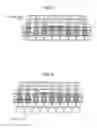
However, in a semiconductor device of chip-on-chip structure, there is a problem that the thickness becomes large, because it has a construction in which IC chips 151 and 152 are simply stacked on a substrate 153 as shown in FIG. 15, for example.
Further, the wiring pattern (not illustrated) formed onto the substrate 153 needs to be connected with the IC chip 151 by a wire 154 made of metal or the like, because the surface of the IC chip 151 on which electrodes are provided does not face the substrate. As a result, when a high-frequency signal is handled in particular, there is also a problem that harmful effects caused by the inductance component of the wire 154 (such as poor sensitivity and varying sensitivity) cannot be ignored.
On the other hand, in Japanese Patent Application Laid-open Publication No. 2002-83925, an integrated circuit device is disclosed asshown in FIG. 16. In the integrated circuit device, a first IC chip 161 and a second IC chip 162 are connected electrically via bumps 163, and a recess 165 enough to accommodate the second IC chip 162 is formed on a surface of a substrate 164. And the first IC chip 161 and the substrate 164 are connected electrically at a position where the second IC chip 162 is situated in the recess 165. In this integrated circuit device, the second IC chip 162 is located inside the recess, and the first IC chip 161 and the substrate 164 are connected without a wire. As a result, thinning can be achieved and the harmful influence by an inductance component which occurs in case of a circuit which handles a high-frequency signal can be reduced.
However, in the integrated circuit device in the above-mentioned Japanese Patent Application, heat tends to be accumulated around the first IC chip 161, and there is a problem that the heat radiation characteristics is not good.
SUMMARY
An exemplary object of the invention is to provide a semiconductor device in which miniaturization is realized, negative effect of an inductance component when handling a high-frequency signal is mitigated, and also heat radiation characteristics is improved.
BRIEF DESCRIPTION OF THE DRAWINGS
Exemplary features and advantages of the present invention will become apparent from the following detailed description when taken with the accompanying drawings in which:
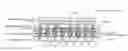
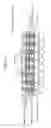
FIG. 1 is a sectional view of a semiconductor device 1 of a first embodiment of the present invention;
FIG. 2 is a diagram showing a production process of a build-up substrate 2;
FIG. 3 is a diagram showing the production process (continuation of FIG. 2) of the build-up substrate 2;
FIG. 4 is a diagram showing the production process (continuation of FIG. 3) of the build-up substrate 2;
FIG. 5 is a diagram showing s mounting process of LSI chips 3 and 4;
FIG. 6 is a diagram showing the mounting process (continuation of FIG. 5) of the LSI chips 3 and 4;
FIG. 7 is a diagram showing the mounting process (continuation of FIG. 6) of the LSI chips 3 and 4;
FIG. 8 is a diagram showing the mounting process (continuation of FIG. 7) of the LSI chips 3 and 4;
FIG. 9 a diagram showing a mounting procesS of BGA balls;
FIG. 10 is a sectional view of a semiconductor device 1 of a second embodiment of the present invention;
FIG. 11 is a sectional view showing a modification example of the semiconductor device 1 according to the first embodiment of the present invention;
FIG. 12 is a sectional view showing a modification example of the semiconductor device 1;
FIG. 13 is a sectional view showing a modification example of the semiconductor device 1 of the first and second embodiment of the present invention;
FIG. 14 is a diagram showing a modification example of the semiconductor device 1;
FIG. 15 is a diagram showing a semiconductor device having some relation with the present invention; and
FIG. 16 is a diagram showing an integrated circuit device having some relation with the present invention.
EXEMPLARY EMBODIMENT
Next, a first exemplary embodiment of the semiconductor device of the present invention will be described.
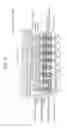
FIG. 1 is a sectional view of the semiconductor device 1 according to this embodiment.
The semiconductor device 1 includes a substrate 2 (hereinafter, referred to as “a package substrate”), a semiconductor element 3 (hereinafter, referred to as “an LSI chip 3”) and a semiconductor element 4 (hereinafter, referred to as “an LSI chip 4”).
A cavity 6 enough to accommodate the LSI chips is formed into the package substrate 2 (In this case, the LSI chip 3 is smaller than the package substrate 2). On the bottom face of the cavity 6, an inner layer conductor 7 of the package substrate 2 is exposed.
The LSI chip 3 is mounted in a face-up manner and is connected with the LSI chip 4 via bumps 5 which are made of gold or the like. Wiring is drawn out from the bumps 5, and the LSI chip 3 is connected with the LSI chip 4 electrically via the wiring. Thermal grease 8 lies between the LSI chip 3 and the inner layer conductor 7 and the LSI chip 3 contacts the inner layer conductor 7 via the thermal grease 8.
The LSI chip 4 is mounted in a face-down manner and connected with the package substrate 2 at a position where the LSI chip 3 can be accommodated in the cavity 6. The LSI chip 3 is connected with the wiring formed on the package substrate 2 electrically via the bumps 5 without a wire.
According to the embodiment, there are effects that the miniaturization of a semiconductor device can be achieved and the harmful influence of an inductance component can be reduced. Also, there is another effect that it is possible to improve the heat radiation characteristics by the LSI chip 3 contacting the inner layer conductor 7 of metal via the thermal grease 8.
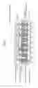
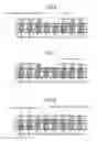
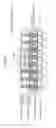
A manufacturing method of the semiconductor device 1 will be described below using FIGS. 2 to 10. Here, although a build-up substrate is described as an example of a package substrate, it is not limited to this.
[Step 1] Production Process of the Build-up Substrate 2 (FIGS. 2-4)
A manufacturing method of the build-up substrate 2 will be described.
First, in FIG. 1, a core substrate 9 is formed using a double-sided copper-clad core material and a prepreg. The core substrate 9 corresponds to the inner layer conductor 7 of FIG. 1. Next, by providing through hole vias 10 and performing outer layer circuit forming using a subtractive process which is common, a core outer layer conductor 11 is formed. The core substrate 9 also has a core inner layer conductor 12 in an inner layer.
Next, in FIG. 3, by forming build-up vias 13 and wiring on both sides of the core substrate 9, a build layer is formed. The build layer formed on the upper surface of the core substrate 9 is called a front build layer 14, and the build layer formed on the under surface of the core substrate 9 is called a back build layer 15.
Then, flip chip bonding pads 16 for mounting a LSI is provided on the outermost surface of the front build layer 14. Also, BGA pads 17 for placing BGA (Ball Grid Array) balls are provided on the outermost surface of the back build layer 15.
Next, in FIG. 4, the cavity 6 is scraped out using a routing machine. At this time, scraping in the depth direction is stopped at a time point when the core outer layer conductor 11 of the core substrate 9 is exposed. As disclosed in the above-mentioned Japanese Patent Application, the precision of the scraping process can be improved by detecting an electrical contact between a cutting drill and an exposed inner layer conductor. When the thickness of the LSI chip 3 is large, the processing may be continued until the core inner layer conductor 12 is exposed.
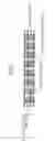
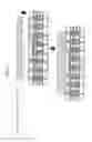
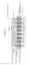
[Step 2] Mounting Process of the LSI chips 3 and 4 (FIGS. 5-8)
First, in FIG. 5, a Proper Quantity of the Thermal grease 8 is applied on the core outer layer conductor 11 in the cavity.
Next, in FIG. 6, the LSI chip 3 is mounted on the thermal grease 8 in a face-up manner. Flip chip bonding pads 18 formed in the same pitch as input terminals of the LSI chip 4 are provided on the circuit side of the LSI chip 3. The back of the LSI chip 3 is polished beforehand and the heights of the flip chip bonding pads 18 and the flip chip bonding pads 16 are adjusted so that they may become the same.
Next, in FIG. 7, solder paste is pre-coated on the flip chip bonding pads 16 of the build-up substrate 2 and the flip chip bonding pads 18 of the LSI chip 3 using a printing method. After that, flip-chip mounting is performed for the LSI chip 4 in a face-down manner.
Next, in FIG. 8, underfill resin 19 is filled between the build-up substrate 2 and the LSI chip 4, also including the cavity 6.
[Step 3] Mounting Process of BGA Balls (FIG. 9)
BGA balls 20 is mounted on the BGA pads 17 of the build-up substrate 2 (refer to FIG. 9).
By the above-mentioned steps, it is possible to produce a semiconductor device in which the harmful effect of an inductance component can be mitigated while realizing miniaturization, and which is capable of improving heat radiation characteristics.
Next, a second embodiment of the semiconductor device of the present invention will be described.
The semiconductor device in the second embodiment has a heat sink for improving heat radiation characteristics in addition to the structure of the first embodiment.
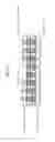
A sectional view of a semiconductor device 11 according to the second embodiment is shown in FIG. 10.
The second embodiment is different from the first embodiment only in the point that a heat sink 22 is attached on the upper surface of the LSI chip 4 via thermal grease 21.
As for the manufacturing method, only a step for applying a proper quantity of the thermal grease 22 on the back surface of the LSI chip 4 and mounting the heat sink 22 on it has to be added after Step 3 in the first embodiment (mounting process of BGA balls).
In the second embodiment, by providing a heat sink, heat radiation characteristics can be further improved.
Meanwhile, when the number of stacked LSI chips which is required is just one in the first embodiment, the device may be constructed such that the flip chip bonding pads 16 of the package substrate 2 and the flip chip bonding pads 18 of the LSI chip 3 are connected electrically via wires, as shown in FIG. 11. When it is desired to set the number of stacked LSI chips to no smaller than two, the construction may be such that a LSI chip having the flip chip bonding pads 18 on its upper and lower surfaces is stacked between the LSI chip 3 and the inner layer conductor 7.
In FIG. 12, an example in which one LSI chip (that is, a LSI chip 24) which has the flip chip bonding pads 18 on its upper and lower surfaces, is stacked between the LSI chip 3 and the inner layer conductor 7. (penetration silicon vias are provided in FIG. 12, but are not shown in FIG. 12)
Further, in the first and second embodiments, when it is desired to set the number of the LSI chips to no smaller than three, the device may be constructed such that a plurality of cavities 6s are provided or additional LSI chips are stacked on the LSI chip 4. In FIG. 13, there is shown an example where one LSI chip 25 is stacked on the LSI chip 4. In this case, a penetration silicon via is provided in the LSI chip 4, although not shown.
In the first and second embodiments, although the thermal grease 8 is being used in order to improve heat radiation characteristics, the construction may be such that, as shown in FIG. 14, the LSI chip 3 contacts the inner layer conductor 7 directly without using the thermal grease 8.
Also, in the first and second embodiments, although the thermal grease 8 is used as a heat conduction material intervening between the LSI chip 3 and the package substrate 2, solder may be used in place of the thermal grease 8. When solder has a thermal conductivity higher than that of thermal grease, heat radiation characteristics can be improved more. Further, in the present invention, although thermal grease and solder has been illustrated, the heat conduction material is not limited to those. It may be anything with a high thermal conductivity.
Further, in the first and second embodiments, a ceramic substrate may be used as the package substrate 2.
Yet further, in the above description of the first and second embodiments, although BGA has been used, LGA (Land Grid Array) may be used instead of BGA.
The previous description of embodiments is provided to enable a person skilled in the art to make and use the present invention. Moreover, various modifications to these exemplary embodiments will be readily apparent to those skilled in the art, and the generic principles and specific examples defined herein may be applied to other embodiments without the use of inventive faculty. Therefore, the present invention is not intended to be limited to the exemplary embodiments described herein but is to be accorded the widest scope as defined by the limitations of the claims and equivalents.
Further, it is noted that the inventor's intent is to retain all equivalents of the claimed invention even if the claims are amended during prosecution.
Claims
1. A manufacturing method of a semiconductor device comprising:
forming a cavity by scraping a substrate, a bottom surface of said cavity being an inner layer conductor which is exposed;
making a first semiconductor element contact, in said cavity, said inner layer conductor directly or via a good heat conduction material; and
connecting a second semiconductor element with said first semiconductor element and said substrate electrically.
2. The manufacturing method of a semiconductor device according to claim 1, wherein
said first semiconductor element is mounted in a face-up manner in said first mounting and said second semiconductor element is mounted a face-down manner in said second mounting.
3. The manufacturing method of a semiconductor device according to claim 2, wherein
said second semiconductor element is mounted in a flip-chip-mounting manner.
4. The manufacturing method of a semiconductor device according to claim 3, wherein said first semiconductor element and said second semiconductor element are connected via bumps.
5. The manufacturing method of a semiconductor device according to claim 1, wherein said good heat conduction material is thermal grease or solder.
6. The manufacturing method of a semiconductor device according to claim 1, further comprising:
mounting a heat sink on an upper surface of said second semiconductor element.
7. The manufacturing method of a semiconductor device according to claim 1, further comprising:
stacking a third semiconductor element between said first and second semiconductor elements before connecting said second semiconductor element with said first semiconductor element and said substrate electrically.
Images & Drawings included:


Sources:
- United States Patent and Trademark Office - verify current appl. status at the USPTO↗
Similar patent applications:
- » 10230423
Semiconductor device manufacturing method, semiconductor device manufacturing apparatus, semiconductor device manufacturing system, and cleaning method for semiconductor device manufacturing apparatus - » 10201720
Semiconductor thin-film manufacturing method, semiconductor device manufacturing method, semiconductor device, integrated circuit, electro-optical device, and electronic appliance - » 20230187203
Semiconductor device manufacturing method, semiconductor memory device manufacturing method, semiconductor memory device, and substrate treatment apparatus - » 20100193792
LAMINATED FILM MANUFACTURING METHOD, SEMICONDUCTOR DEVICE MANUFACTURING METHOD, SEMICONDUCTOR DEVICE AND DISPLAY DEVICE - » 10739275
Wafer flatness evaluation method, wafer flatness evaluation apparatus carrying out the evaluation method, wafer manufacturing method using the evaluation method, wafer quality assurance method using the evaluation method, semiconductor device manufacturing method using the evaluation method and semiconductor device manufacturing method using a wafer evaluated by the evaluation method - » 20090214964
Semiconductor device manufacturing method, semiconductor device manufacturing equipment, and computer readable medium - » 20070177127
Wafer flatness evaluation method, wafer flatness evaluation apparatus carrying out the evaluation method, wafer manufacturing method using the evaluation method, wafer quality assurance method using the evaluation method, semiconductor device manufacturing method using the evaluation method and semiconductor device manufacturing method using a wafer evaluated by the evaluation method - » 20070090093
Semiconductor device manufacturing method, semiconductor device manufacturing apparatus, control program and computer storage medium - » 20070177126
Wafer flatness evaluation method, wafer flatness evaluation apparatus carrying out the evaluation method, wafer manufacturing method using the evaluation method, wafer quality assurance method using the evaluation method, semiconductor device manufacturing method using the evaluation method and semiconductor device manufacturing method using a wafer evaluated by the evaluation method - » 20090032950
Film forming method, semiconductor device manufacturing method, semiconductor device, program and recording medium
Recent applications in this class:
- » 20250293212 2025-09-18
SEMICONDUCTOR PACKAGES - » 20250293211 2025-09-18
HEAT DISSIPATION FOR STACKED INTEGRATED CIRCUIT DEVICES - » 20250293210 2025-09-18
SYSTEMS AND METHODS FOR PACKAGING A SEMICONDUCTOR DEVICE - » 20250286021 2025-09-11
SEMICONDUCTOR PACKAGE - » 20250286020 2025-09-11
SEMICONDUCTOR BONDING STRUCTURE - » 20250286019 2025-09-11
SEMICONDUCTOR PACKAGE - » 20250286018 2025-09-11
METHOD OF FABRICATING SEMICONDUCTOR BONDING STRUCTURE - » 20250286017 2025-09-11
SEMICONDUCTOR DEVICE - » 20250279399 2025-09-04
SEMICONDUCTOR DEVICES AND MANUFACTURING METHODS OF THE SAME - » 20250279398 2025-09-04
VERTICAL INTERCONNECT STRUCTURES IN THREE-DIMENSIONAL INTEGRATED CIRCUITS
Recent applications for this Assignee:
- » 20250295043 2025-09-18
SUPERCONDUCTING QUANTUM CIRCUIT - » 20250294700 2025-09-18
ELECTRONIC DEVICE RACK, ELECTRONIC DEVICE UNIT, AND METHOD OF INSTALLING ELECTRONIC DEVICE RACK - » 20250294570 2025-09-18
RADIO ACCESS NETWORK NODE, RADIO TERMINAL, AND METHODS AND NON-TRANSITORY COMPUTER-READABLE MEDIA THEREFOR - » 20250294518 2025-09-18
MONITORING DEVICE, TRACKING METHOD, AND NON-TRANSITORY COMPUTER-READABLE MEDIUM - » 20250294486 2025-09-18
METHOD, DEVICE AND COMPUTER READABLE MEDIUM FOR COMMUNICATIONS - » 20250294444 2025-09-18
CELL SELECTION BASED ON USER CAPABILITY - » 20250293871 2025-09-18
PRIVATE KEY RECOVERY DEVICE, PRIVATE KEY RECOVERY METHOD, AND STORAGE MEDIUM - » 20250293866 2025-09-18
QUANTUM KEY DISTRIBUTION SYSTEM, KEY MANAGEMENT APPARATUS, AND KEY MANAGEMENT METHOD - » 20250293833 2025-09-18
METHODS, DEVICES, AND COMPUTER READABLE MEDIUM FOR COMMUNICATION - » 20250293791 2025-09-18
COMMUNICATION CONTROL APPARATUS, COMMUNICATION APPARATUS, COMMUNICATION SYSTEM, STORAGE MEDIUM, AND COMMUNICATION CONTROL METHOD