IMEC VZW
Leuven
Belgium
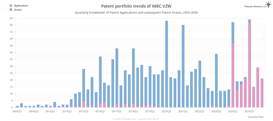
996
2026-04-02
955
2026-01-13
Top Inventors for applications by IMEC VZW
These are the the leading inventors for applications assigned to IMEC VZW:
- Julien Ryckaert 29 Schaerbeek, Belgium
- Boon Teik Chan 25 Wilsele, Belgium
- Jan Craninckx 25 Boutersem, Belgium
- Juergen Boemmels 21 Heverlee, Belgium
- Boon Teik Chan 21 Leuven, Belgium
- Xavier Rottenberg 21 Kessel-lo, Belgium
- Pol Van Dorpe 21 Spalbeek, Belgium
- Eric Beyne 19 Heverlee, Belgium
- Liesbet Lagae 19 Leuven, Belgium
- Peter Peumans 19 Herfelingen, Belgium
- Francky Catthoor 19 Temse, Belgium
- Jan VAN HOUDT 16 Bekkevoort, Belgium
- Abdulkadir YURT 16 Heverlee, Belgium
- Geert Vanmeerbeeck 16 Keerbergen, Belgium
- Naoto Horiguchi 16 Leuven, Belgium
- Nadine Collaert 15 Blanden, Belgium
- Tim Stakenborg 15 Heverlee, Belgium
- Richard Stahl 15 Rotselaar, Belgium
- Geert Van Der Plas 14 Leuven, Belgium
- Zheng Tao 14 Heverlee, Belgium
- Bernardette Kunert 14 Wilsele, Belgium
- Gouri Sankar KAR 13 Leuven, Belgium
- Clement Merckling 13 Evere, Belgium
- Simone Severi 12 Leuven, Belgium
- Zsolt Tokei 12 Leuven, Belgium
- Efrain Altamirano Sanchez 12 Kessel-lo, Belgium
- Gaspard Hiblot 12 Leuven, Belgium
- Ewout Martens 11 Heverlee, Belgium
- Johan Swerts 11 Kessel-lo, Belgium
- Paolo Fiorini 11 Brussels, Belgium
- Liesbeth Witters 11 Lubbeek, Belgium
- Benjamin Jones 11 Kessel-Lo, Belgium
- Amey Mahadev Walke 11 Heverlee, Belgium
- Frederic Lazzarino 10 Hamme-Mille, Belgium
- Hanns Christoph Adelmann 10 Wilsele, Belgium
- Anabela Veloso 10 Leuven, Belgium
- André Bourdoux 10 Theux, Belgium
- Roeland Baets 10 Deinze, Belgium
- Ziduo Lin 10 Heverlee, Belgium
- Philippe Vereecken 9 Liege, Belgium
- Sebastien Couet 9 Grez-Doiceau, Belgium
- STEVEN DEMUYNCK 9 AARSCHOT, Belgium
- Willem Van Roy 9 Bierbeek, Belgium
- Jan GENOE 9 Testelt, Belgium
- Trong Huynh Bao 9 Leuven, Belgium
- Geoffrey Pourtois 9 Villers-la-Ville, Belgium
- Wim BOGAERTS 9 Melle, Belgium
- Maarten Rosmeulen 9 Ghent, Belgium
- Dries Vercruysse 9 Sint Andries, Belgium
- Hans Mertens 9 Leuven, Belgium
- Maarten Rosmeulen 9 Gent, Belgium
- Andy Lambrechts 9 Herent, Belgium
- Benjamin HERSHBERG 8 Leuven, Belgium
- Emily Gallagher 8 Burlington, VT United States
- Chengxun Liu 8 Kessel-Lo, Belgium
- Kris Myny 8 Heusden-Zolder, Belgium
- Veronique ROCHUS 8 Leuven, Belgium
- Eugenio Dentoni Litta 8 Leuven, Belgium
- Paolo Fiorini 8 Brussel, Belgium
- Joris Van Campenhout 8 Brussel, Belgium
- Peter BIENSTMAN 8 Gent, Belgium
- Cedric Huyghebaert 8 Heverlee, Belgium
- Kurt Wostyn 8 Lubbeek, Belgium
- Joris Van Campenhout 8 Brussels, Belgium
- Pieter Weckx 8 Bunsbeek, Belgium
- Tom CLAES 8 Merelbeke, Belgium
- Roel GRONHEID 7 Huldenberg, Belgium
- Silvia Armini 7 Heverlee, Belgium
- Praveen Raghavan 7 Leefdaal, Belgium
- Basoene Briggs 7 Heverlee, Belgium
- David Cheyns 7 Heffen, Belgium
- Pierre Wambacq 7 Groot-Bijgaarden, Belgium
- Geert Hellings 7 Halle, Belgium
- Niamh Waldron 7 Heverlee, Belgium
- Peter Bienstman 7 Ghent, Belgium
- Stefan Cosemans 7 Leuven, Belgium
- Gunther Roelkens 6 Schellebelle, Belgium
- Florin Ciubotaru 6 Heverlee, Belgium
- Geert Eneman 6 Balen, Belgium
- Kristof Paredis 6 Oud-Heverlee, Belgium
- Steve Stoffels 6 Haasrode, Belgium
- Bogdan GOVOREANU 6 Hulshout, Belgium
- Mohit Gupta 6 Heverlee, Belgium
- Roelof Jansen 6 Heverlee, Belgium
- Sushil Sakhare 6 Heverlee, Belgium
- Robert Gehlhaar 6 Herent, Belgium
- Maarten Mees 6 Kessel-Lo, Belgium
- Wilfried VANDERVORST 6 Mechelen, Belgium
- Hendrik F.W. Dekkers 6 Tienen, Belgium
- Alessio Spessot 6 Heverlee, Belgium
- Manu Komalan Perumkunnil 6 Leuven, Belgium
- Ashwyn Srinivasan 6 Heverlee, Belgium
- Jonathan Borremans 6 Lier, Belgium
- Christopher Wilson 6 Tervuren, Belgium
- Geert Eneman 6 Heverlee, Belgium
- Hendrik F. W. Dekkers 5 Tienen, Belgium
- Guy Torfs 5 Gent, Belgium
- Dries Van Thourhout 5 Gent, Belgium
- Yves Mols 5 Wijnegem, Belgium
- Marina Timmermans 5 Bertem, Belgium
Recent patent applications by IMEC VZW
IMEC VZW based in Leuven, BE has been assigned the rights to these inventions. The list includes both Pending Applications and Patent Grants:
US20260094270A1
PhysicsMETHODS AND SYSTEMS FOR DETERMINING AN ANATOMICAL RECONSTRUCTION OF A BROKEN BONE
#2 | 2025-06-19 ✅ Patent 12,527,094 granted on 2026-01-13US20250204055A1
ElectricityBYPASS DIODE ASSEMBLY FOR A PHOTOVOLTAIC MODULE AND METHOD FOR FABRICATING
#3 | 2025-06-19US20250199418A1
PhysicsMEASURING CONTRAST AND CRITICAL DIMENSION USING AN ALIGNMENT SENSOR
#4 | 2025-03-20 ✅ Patent 12,635,263 granted on 2026-05-19US20250098336A1
ElectricityTECHNICAL WEAVE FOR PHOTOVOLTAIC MODULES
#5 | 2024-11-21 ✅ Patent 12,613,276 granted on 2026-04-28US20240385243A1
PhysicsPHOTONIC WAVEGUIDE POWER AND PHASE MONITOR
#6 | 2024-09-05 ✅ Patent 12,558,270 granted on 2026-02-24US20240293266A1
Human necessitiesSENSING DIAPER CONTENT
#7 | 2024-08-29 ✅ Patent 12,544,216 granted on 2026-02-10US20240285394A1
Human necessitiesARTIFICIAL IRIS, A METHOD FOR CONTROLLING AN ARTIFICIAL IRIS, AN ARTIFICIAL IRIS, A METHOD FOR CONTROLLING AN ARTIFICIAL IRIS, AND A METHOD FOR DETERMINING A USER-SPECIFIC PROFILE FOR AN ARTIFICIAL IRIS AND A METHOD FOR DETERMINING A USER-SPECIFIC PROFILE FOR AN ARTIFICIAL IRIS
#8 | 2024-08-22 ✅ Patent 12,627,298 granted on 2026-05-12US20240283457A1
ElectricityCIRCUITRY AND A METHOD FOR GENERATING A SET OF OUTPUT CLOCK SIGNALS
#9 | 2024-08-08 ✅ Patent 12,471,862 granted on 2025-11-18US20240260915A1
Human necessitiesA PHASE-CONTRAST X-RAY IMAGING SYSTEM FOR OBTAINING A DARK-FIELD IMAGE AND A METHOD THEREFOR
#10 | 2024-07-11 ✅ Patent 12,631,934 granted on 2026-05-19US20240231174A9
PhysicsMach-Zehnder-Interferometer Filter and Ring-Based Wavelength-Demultiplexing Device
#11 | 2024-07-11US20240229217A9
Chemistry; metallurgyA METHOD FOR ETCHING MOLYBDENUM
#12 | 2024-07-04 ✅ Patent 12,618,752 granted on 2026-05-05US20240219272A1
PhysicsA COLLECTING DEVICE AND A METHOD FOR COLLECTION OF AIRBORNE PARTICLES EXHALED BY A HUMAN BEING
#13 | 2024-06-27 ✅ Patent 12,462,880 granted on 2025-11-04US20240212763A1
PhysicsMatrix-Vector Multiplications Based on Charge-Summing Memory Cell Strings
#14 | 2024-06-27 ✅ Patent 12,429,660 granted on 2025-09-30US20240210641A1
PhysicsImaging Device, an Imaging System and a Method for Wavelength Dependent Imaging
#15 | 2024-06-20 ✅ Patent 12,607,605 granted on 2026-04-21US20240201138A1
PhysicsSENSOR DEVICE, A PHOTO-ACOUSTIC IMAGING DEVICE AND A METHOD FOR DETECTING A MEASURAND
#16 | 2024-06-20 ✅ Patent 12,194,497 granted on 2025-01-14US20240198382A1
Performing operations; transportingFlexible ultrasound transducer
#17 | 2024-05-30 ✅ Patent 12,542,562 granted on 2026-02-03US20240178855A1
ElectricityINPUT BUFFER AND A METHOD FOR REDUCING A SIGNAL AMPLITUDE DEPENDENCY OF SAID INPUT BUFFER
#18 | 2024-05-30 ✅ Patent 12,584,943 granted on 2026-03-24US20240175896A1
PhysicsMethod for Producing a Substrate Comprising Multiple Tips for Scanning Probe Microscopy
#19 | 2024-05-23 ✅ Patent 12,592,277 granted on 2026-03-31US20240170051A1
PhysicsDISTRIBUTED WRITE DRIVER FOR MEMORY ARRAY
#20 | 2024-05-23 ✅ Patent 12,531,100 granted on 2026-01-20US20240170034A1
PhysicsWRITE-READ CIRCUIT WITH A BIT LINE MULTIPLEXER FOR A MEMORY DEVICE
#21 | 2024-05-09 ✅ Patent 12,379,613 granted on 2025-08-05US20240151990A1
PhysicsElectro-Optical Component
#22 | 2024-04-25US20240133016A1
Chemistry; metallurgyA METHOD FOR ETCHING MOLYBDENUM
#23 | 2024-04-18 ✅ Patent 12,648,213 granted on 2026-06-02US20240128124A1
ElectricityMETHODS FOR FORMING STACKED TRANSISTOR DEVICES
#24 | 2024-04-18 ✅ Patent 12,618,152 granted on 2026-05-05US20240124975A1
Chemistry; metallurgyMETHOD OF DEPOSITING A TRANSITION METAL DICHALCOGENIDE
#25 | 2024-04-11 ✅ Patent 12,342,503 granted on 2025-06-24US20240121914A1
ElectricityDEVICE AND SYSTEM FOR COOLING AN ELECTRONIC COMPONENT
#26 | 2024-04-11 ✅ Patent 12,374,392 granted on 2025-07-29US20240119998A1
Physics3D Integrated Circuit
#27 | 2024-04-04 ✅ Patent 12,406,732 granted on 2025-09-02US20240112737A1
PhysicsMETHOD OF PROGRAMMING FLASH MEMORY
#28 | 2024-03-07 ✅ Patent 12,392,714 granted on 2025-08-19US20240077411A1
PhysicsOPTICAL ALIGNMENT COMPENSATION SYSTEM FOR A GAS DETECTION SYSTEM
#29 | 2024-02-01 ✅ Patent 12,206,413 granted on 2025-01-21US20240039541A1
ElectricitySFQ-based pulse-conserving logic gates
#30 | 2024-02-01 ✅ Patent 12,431,389 granted on 2025-09-30US20240038589A1
ElectricitySUPERCONDUCTIVE INTERCONNECT STRUCTURE
#31 | 2024-02-01 ✅ Patent 12,094,530 granted on 2024-09-17US20240038298A1
PhysicsJosephson static random access memory
#32 | 2024-02-01 ✅ Patent 12,204,025 granted on 2025-01-21US20240036199A1
PhysicsMethod and a device for determining a distance to a target
#33 | 2024-01-18 ✅ Patent 12,542,282 granted on 2026-02-03US20240021837A1
ElectricityCOATED THREE-DIMENSIONAL ELECTRONICALLY CONDUCTIVE NETWORK
#34 | 2024-01-18 ✅ Patent 12,428,749 granted on 2025-09-30US20240018686A1
Chemistry; metallurgyTEMPLATE FOR GROWING A CRYSTAL OF A TWO-DIMENSIONAL MATERIAL
#35 | 2024-01-11 ✅ Patent 12,519,547 granted on 2026-01-06US20240014906A1
ElectricityPHOTONIC MACHINE LEARNING BASED SIGNAL RECOVERY IN SELF-COHERENT DETECTORS
#36 | 2024-01-04 ✅ Patent 12,237,207 granted on 2025-02-25US20240006228A1
ElectricityMethod for forming a buried metal line in a semiconductor substrate
#37 | 2023-12-28 ✅ Patent 12,635,211 granted on 2026-05-19US20230420544A1
ElectricityMETHOD OF FORMING A SEMICONDUCTOR DEVICE
#38 | 2023-12-21 ✅ Patent 12,513,878 granted on 2025-12-30US20230413505A1
ElectricityBit Cell with Isolating Wall
#39 | 2023-12-07 ✅ Patent 12,648,165 granted on 2026-06-02US20230395561A1
ElectricityMethod for Producing a Semiconductor Chip
#40 | 2023-12-07 ✅ Patent 12,480,814 granted on 2025-11-25US20230392984A1
PhysicsDEVICE AND A METHOD FOR POLARIZATION DEPENDENT IMAGING
#41 | 2023-11-30 ✅ Patent 12,484,289 granted on 2025-11-25US20230386928A1
ElectricityMethod for Forming a Stacked Transistor Device
#42 | 2023-11-23 ✅ Patent 12,474,207 granted on 2025-11-18US20230375406A1
PhysicsLIGHT SENSOR AND A METHOD FOR MANUFACTURING A LIGHT SENSOR
#43 | 2023-11-09 ✅ Patent 12,446,247 granted on 2025-10-14US20230361205A1
ElectricityCircuit cell for a standard cell semiconductor device
#44 | 2023-10-26 ✅ Patent 12,368,451 granted on 2025-07-22US20230344441A1
ElectricitySLOPE ANALOG-TO-DIGITAL CONVERTER, A SYSTEM AND A METHOD FOR CONVERTING AN ANALOG INPUT SIGNAL TO A DIGITAL REPRESENTATION
#45 | 2023-10-19 ✅ Patent 12,602,070 granted on 2026-04-14US20230333584A1
PhysicsVOLTAGE REFERENCE CIRCUIT AND A POWER MANAGEMENT UNIT
#46 | 2023-10-19 ✅ Patent 12,306,649 granted on 2025-05-20US20230333580A1
PhysicsReference circuit and a power management unit
#47 | 2023-10-05 ✅ Patent 12,468,327 granted on 2025-11-11US20230315137A1
PhysicsA VOLTAGE REFERENCE CIRCUIT AND A POWER MANAGEMENT UNIT
#48 | 2023-10-05 ✅ Patent 12,279,911 granted on 2025-04-22US20230309966A1
Human necessitiesUltrasound transducer and a system
#49 | 2023-09-28 ✅ Patent 12,500,062 granted on 2025-12-16US20230307207A1
ElectricityA RECONSTRUCTION METHOD FOR ATOM PROBE TOMOGRAPHY
#50 | 2023-09-21 ✅ Patent 12,255,408 granted on 2025-03-18US20230299478A1
ElectricityPhased array transceiver element
#51 | 2023-09-21 ✅ Patent 12,419,132 granted on 2025-09-16US20230299226A1
ElectricityMethod for Interconnecting Photovoltaic Cells and Photovoltaic Cell Assembly
#52 | 2023-09-21 ✅ Patent 12,620,550 granted on 2026-05-05US20230298854A1
ElectricityMETHOD OF PERFORMING METROLOGY ON A MICROFABRICATION PATTERN
#53 | 2023-09-14 ✅ Patent 12,456,641 granted on 2025-10-28US20230290664A1
ElectricityMethod for Positioning Components on a Substrate and Substrates Suitable for the Method
#54 | 2023-09-14 ✅ Patent 12,626,481 granted on 2026-05-12US20230290107A1
PhysicsLIGHT FIELD RENDERING
#55 | 2023-09-14 ✅ Patent 12,385,813 granted on 2025-08-12US20230288299A1
PhysicsELECTRON MICROSCOPY GRIDS AND HIGH-RESOLUTION STRUCTURAL DETERMINATION METHODS
#56 | 2023-09-07 ✅ Patent 12,436,030 granted on 2025-10-07US20230280208A1
PhysicsDetector for Detecting Electromagnetic Radiation, Image Sensor, and Method for Detecting Image Information
#57 | 2023-08-31 ✅ Patent 12,301,242 granted on 2025-05-13US20230275593A1
ElectricityAnalog-to-digital converter circuit
#58 | 2023-08-24 ✅ Patent 12,317,756 granted on 2025-05-27US20230270020A1
ElectricitySuperconducting chip package with improved magnetic shielding
#59 | 2023-08-17 ✅ Patent 12,041,782 granted on 2024-07-16US20230262990A1
ElectricityMemory device with ferroelectric charge trapping layer
#60 | 2023-06-29 ✅ Patent 12,512,417 granted on 2025-12-30US20230207482A1
ElectricityMethod and Structure for Determining an Overlay Error
#61 | 2023-06-29 ✅ Patent 12,424,276 granted on 2025-09-23US20230206996A1
PhysicsMULTIPORT MEMORY CELLS INCLUDING STACKED ACTIVE LAYERS
#62 | 2023-06-29 ✅ Patent 12,440,667 granted on 2025-10-14US20230201573A1
Human necessitiesMethod for Manufacturing an Electrode
#63 | 2023-06-22 ✅ Patent 12,414,302 granted on 2025-09-09US20230200078A1
ElectricityFerroelectric Device
#64 | 2023-06-22 ✅ Patent 12,289,117 granted on 2025-04-29US20230198543A1
ElectricityInput circuitry and a method for receiving an analog input signal
#65 | 2023-06-22 ✅ Patent 12,191,880 granted on 2025-01-07US20230198539A1
ElectricitySlope analog-to-digital converter and a method for analog-to-digital conversion of an analog input signal
#66 | 2023-06-22 ✅ Patent 12,520,556 granted on 2026-01-06US20230197831A1
ElectricityMethod for Forming a Semiconductor Device
#67 | 2023-06-22 ✅ Patent 12,457,785 granted on 2025-10-28US20230197830A1
ElectricityMethod for Forming a Stacked FET Device
#68 | 2023-06-22 ✅ Patent 12,439,673 granted on 2025-10-07US20230197807A1
ElectricitySplit Gate FerroFET
#69 | 2023-06-22 ✅ Patent 12,532,555 granted on 2026-01-20US20230197761A1
ElectricityMethod for Producing a Multipixel Detector
#70 | 2023-06-22 ✅ Patent 12,527,079 granted on 2026-01-13US20230197726A1
ElectricityMethod for Forming a Stacked FET Device
#71 | 2023-06-22 ✅ Patent 12,519,015 granted on 2026-01-06US20230197528A1
ElectricityVIA FORMATION IN AN INTEGRATED CIRCUIT
#72 | 2023-06-22 ✅ Patent 12,610,801 granted on 2026-04-21US20230197514A1
ElectricityMetallization Process for an Integrated Circuit
#73 | 2023-06-22 ✅ Patent 12,334,276 granted on 2025-06-17US20230197353A1
ElectricityMETHOD FOR FORMING OF PEROVSKITE-BASED OPTOELECTRONIC DEVICES
#74 | 2023-06-22 ✅ Patent 12,462,179 granted on 2025-11-04US20230196166A1
PhysicsQubit Device
#75 | 2023-06-22 ✅ Patent 12,189,109 granted on 2025-01-07US20230194844A1
PhysicsLight distribution device, illumination system and imaging system for imaging of samples within microscopy
#76 | 2023-06-22 ✅ Patent 12,130,472 granted on 2024-10-29US20230194781A1
PhysicsMultilevel coupling for phase front engineering
#77 | 2023-06-22 ✅ Patent 12,429,649 granted on 2025-09-30US20230194780A1
PhysicsIntegrated Optical Structure for Multiplexing and/or Demultiplexing
#78 | 2023-06-22 ✅ Patent 12,044,882 granted on 2024-07-23US20230194777A1
PhysicsMultilayer integrated photonic structure
#79 | 2023-06-22 ✅ Patent 12,529,758 granted on 2026-01-20US20230194656A1
PhysicsRadar Transceiver and Antenna Sharing Method Thereof
#80 | 2023-06-15 ✅ Patent 12,563,761 granted on 2026-02-24US20230187539A1
ElectricityVertically Stacked Transistor Structures
#81 | 2023-06-08 ✅ Patent 12,476,727 granted on 2025-11-18US20230179315A1
ElectricityMethod for Disseminating Scaling Information and Application Thereof in VLSI Implementation of Fixed-Point FFT
#82 | 2023-06-08 ✅ Patent 12,446,246 granted on 2025-10-14US20230178640A1
ElectricityFIELD-EFFECT TRANSISTOR DEVICE
#83 | 2023-06-08 ✅ Patent 12,557,378 granted on 2026-02-17US20230178554A1
ElectricityComplementary Field-Effect Transistor Device
#84 | 2023-06-08 ✅ Patent 12,494,424 granted on 2025-12-09US20230178478A1
ElectricityINTERCONNECT STRUCTURE OF A SEMICONDUCTOR COMPONENT AND METHODS FOR PRODUCING THE STRUCTURE
#85 | 2023-06-08 ✅ Patent 12,462,859 granted on 2025-11-04US20230178131A1
PhysicsFree-layer Design for a Voltage Control of Magnetic Anisotropy Magnetic Random Access Memory Device
#86 | 2023-06-08 ✅ Patent 12,399,071 granted on 2025-08-26US20230175899A1
PhysicsCompressible Electrode
#87 | 2023-06-01 ✅ Patent 12,451,429 granted on 2025-10-21US20230170300A1
ElectricityInterconnection Structure for a Semiconductor Device
#88 | 2023-06-01 ✅ Patent 12,381,116 granted on 2025-08-05US20230170255A1
ElectricityInterconnection Structure for a Semiconductor Device
#89 | 2023-05-25 ✅ Patent 12,527,229 granted on 2026-01-13US20230165159A1
ElectricityThermally Stable Spin Orbit Torque Layer for an MRAM Device
#90 | 2023-05-18 ✅ Patent 12,374,675 granted on 2025-07-29US20230154914A1
ElectricityMETHOD OF PRODUCING HYBRID SEMICONDUCTOR WAFER
#91 | 2023-05-18 ✅ Patent 12,517,056 granted on 2026-01-06US20230152233A1
PhysicsWAVEGUIDE WITH SOLID MICRO-EXTRACTION PHASE FOR RAMAN SPECTROSCOPY
#92 | 2023-05-18 ✅ Patent 11,819,864 granted on 2023-11-21US20230149965A1
Performing operations; transportingMethod and an apparatus for applying thin film material onto a substrate
#93 | 2023-05-11 ✅ Patent 12,327,578 granted on 2025-06-10US20230145983A1
PhysicsMAGNETIC DOMAIN WALL-BASED MEMORY DEVICE WITH TRACK-CROSSING ARCHITECTURE
#94 | 2023-05-11 ✅ Patent 11,827,992 granted on 2023-11-28US20230144037A1
Chemistry; metallurgyTransforming a valve metal layer into a template comprising a plurality of spaced (nano)channels and forming spaced structures therein
#95 | 2023-05-11 ✅ Patent 12,362,236 granted on 2025-07-15US20230142597A1
ElectricityMETHOD OF PRODUCING AN INTEGRATED CIRCUIT CHIP INCLUDING A BACK-SIDE POWER DELIVERY NETWORK
#96 | 2023-04-27 ✅ Patent 12,595,168 granted on 2026-04-07US20230127645A1
Performing operations; transportingMethod for Manufacturing a Microfluidic Device
#97 | 2023-04-20 ✅ Patent 12,464,805 granted on 2025-11-04US20230121515A1
ElectricityMethod for Forming an Interconnection Structure
#98 | 2023-03-16 ✅ Patent 12,557,634 granted on 2026-02-17US20230080522A1
ElectricityINTEGRATED CIRCUIT CHIP INCLUDING BACK SIDE POWER DELIVERY TRACKS
#99 | 2023-03-02 ✅ Patent 12,259,361 granted on 2025-03-25US20230067864A1
PhysicsSystem and method for photoacoustic inspection of an object
#100 | 2023-02-16 ✅ Patent 12,538,779 granted on 2026-01-27US20230046117A1
ElectricityMethod for Producing a Buried Interconnect Rail of an Integrated Circuit Chip
Also check out IMEC vzw's (Leuven, Belgium) applicant profile with 1,194 patent applications submitted.
13243 ⎘