AMKOR TECHNOLOGY, INC.
Chandler, Arizona
United States
425
2016-06-30
423
2018-09-18
Top Inventors for applications by AMKOR TECHNOLOGY, INC.
These are the the leading inventors for applications assigned to AMKOR TECHNOLOGY, INC.:
- Ronald Patrick Huemoeller 54 Chandler, AZ United States
- Sukianto Rusli 41 Phoenix, AZ United States
- David Jon Hiner 28 Chandler, AZ United States
- Thomas P. Glenn 19 Gilbert, AZ United States
- Roger D. St. Amand 16 Tempe, AZ United States
- Jeffrey Alan Miks 16 Chandler, AZ United States
- Bob Shih-Wei Kuo 15 Chandler, AZ United States
- Christopher J. Berry 15 Chandler, AZ United States
- Christopher M. Scanlan 14 Chandler, AZ United States
- Akito Yoshida 14 Chandler, AZ United States
- Seong Min Seo 13 Seoul, South Korea
- Steven Webster 13 Chandler, AZ United States
- Ronald Patrick Huemoeller 12 Gilbert, AZ United States
- Young Suk Chung 11 Seoul, South Korea
- Vladimir Perelman 10 Fremont, CA United States
- Jong Sik PAEK 9 Seoul, South Korea
- Ki Wook LEE 9 Seoul, South Korea
- Yeon Ho Choi 8 Chandler, AZ United States
- Gi Jeong Kim 8 Guri-si, South Korea
- Young Wook Heo 8 Phoenix, AZ United States
- Donald Craig Foster 8 Mesa, AZ United States
- Glenn A. Rinne 7 Apex, NC United States
- Mahmoud Dreiza 7 Phoenix, AZ United States
- Jae-Dong KIM 7 Seoul, South Korea
- Yoon Joo Kim 7 Seoul, South Korea
- David Razu 7 Gilbert, AZ United States
- Min Yoo 7 Seoul, South Korea
- Robert Francis Darveaux 7 Higley, AZ United States
- David Bolognia 7 Scottsdale, AZ United States
- Ludovico E. Bancod 7 Chandler, AZ United States
- Robert F. Darveaux 7 Higley, AZ United States
- Doo Hyun Park 6 Gyeonggi-do, South Korea
- Bong-Chan Kim 6 Seongnam-si, South Korea
- Jin Young KIM 6 Seoul, South Korea
- Sang Jae Jang 6 Gwangjin-gu, South Korea
- Sung Su PARK 6 Seoul, South Korea
- Dae Keun Park 5 Seoul, South Korea
- Jeffrey A. Miks 5 Chandler, AZ United States
- Byong Jin Kim 5 Gyeonggi-do, South Korea
- Jun Young Yang 5 Seoul, South Korea
- Miguel Angel Jimarez 5 Gilbert, AZ United States
- Christopher John Berry 5 Chandler, AZ United States
- Robert Lanzone 5 Chandler, AZ United States
- Timothy L. Olson 5 Phoenix, AZ United States
- Sang Hyun Ryu 5 Seoul, South Korea
- Wan Jong Kim 5 Goyang-si, South Korea
- Roy Dale Hollaway 5 Chandler, AZ United States
- Ju Hoon Yoon 5 Seoul, South Korea
- Terry W. Davis 5 Gilbert, AZ United States
- Michael Barrow 5 Chandler, AZ United States
- Curtis Michael Zwenger 5 Chandler, AZ United States
- Vincent DiCaprio 5 Mesa, AZ United States
- Robert Francis DARVEAUX 5 Gilbert, AZ United States
- Kwang Seok Oh 4 Seoul, South Korea
- Choon Heung Lee 4 Kyounggi-do, South Korea
- Hyung Ju LEE 4 Seoul, South Korea
- WanJong Kim 4 Goyang-si, South Korea
- Young Ho Kim 4 Seoul, South Korea
- Ludovico Bancod 4 Chandler, AZ United States
- GiJeong Kim 4 Guri-si, South Korea
- Eun Sook Sohn 4 Seoul, South Korea
- Michael G. Kelly 4 Queen Creek, AZ United States
- Kenneth Kaskoun 4 Phoenix, AZ United States
- Russ Lie 4 Phoenix, AZ United States
- David Hiner 4 Chandler, AZ United States
- Kyu Won LEE 4 Seoul, South Korea
- Choon Heung LEE 4 Seoul, South Korea
- Yoon Joo Kim 4 Nowon-gu, South Korea
- Ji Young Chung 4 Gunpo-si, South Korea
- Sung Sik Jang 4 Hanam-shi, South Korea
- Ravi Kiran Chilukuri 4 Cary, NC United States
- Jae Hun Ku 4 Seoul, South Korea
- Sang-ho LEE 4 Seoul, South Korea
- Jong Sik Paek 4 Incheon, South Korea
- Won Chul Do 4 Seoul, South Korea
- Ahmer Syed 4 Chandler, AZ United States
- Jae Yoon Kim 4 Gangdong-gu, South Korea
- Jong-wook PARK 4 Seoul, South Korea
- Faheem F. Faheem 3 Chandler, AZ United States
- Sung Jin Yang 3 Gangnam-gu, South Korea
- Paul Robert Hoffman 3 Chandler, AZ United States
- YeonHo Choi 3 Chandler, AZ United States
- Paul R. Hoffman 3 Chandler, AZ United States
- Mu Hwan Seo 3 Aspen Heights, Singapore
- Bong-Chan Kim 3 Gyeonggi-do, South Korea
- John A. Miranda 3 Chandler, AZ United States
- Ju Hoon Yoon 3 Gyeonggi-do, South Korea
- Tae Kyung Hwang 3 Seoul, South Korea
- Donald C. Foster 3 Mesa, AZ United States
- Jong Sik Paek 3 Gyeonggi-do, South Korea
- Kyoung Yeon Lee 3 Gyeonggi-do, South Korea
- Jin Seong Kim 3 Seoul, South Korea
- Brett Arnold Dunlap 3 Queen Creek, AZ United States
- Choon Heung Lee 3 Gwangju, South Korea
- Sundeep Nand NANGALIA 3 Raleigh, NC United States
- Ho Cheol Jang 3 Seoul, South Korea
- Christopher Marc Scanlan 3 Chandler, AZ United States
- William M. Anderson 3 Gilbert, AZ United States
- Nozad O. Karim 3 Chandler, AZ United States
- Richard L. Groover 3 Chandler, AZ United States
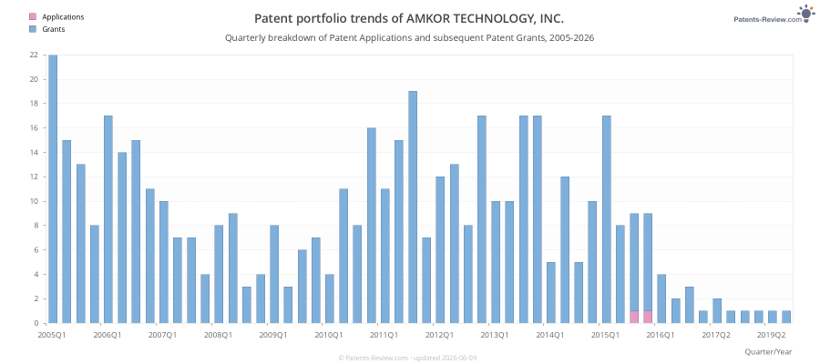
Recent patent applications by AMKOR TECHNOLOGY, INC.
AMKOR TECHNOLOGY, INC. based in Chandler, US has been assigned the rights to these inventions. The list includes both Pending Applications and Patent Grants:
US20160189980A1
ElectricitySemiconductor device and manufacturing method thereof
#2 | 2015-11-26 ✅ Patent 9,875,980 granted on 2018-01-23US20150340332A1
ElectricityCopper pillar sidewall protection
#3 | 2015-10-22US20150303170A1
ElectricitySINGULATED UNIT SUBSTRATE FOR A SEMICONDCUTOR DEVICE
#4 | 2015-08-06US20150221570A1
ElectricityTHIN SANDWICH EMBEDDED PACKAGE
#5 | 2015-05-21 ✅ Patent 9,799,592 granted on 2017-10-24US20150137384A1
ElectricitySemicondutor device with through-silicon via-less deep wells
#6 | 2015-05-12 ✅ Patent 9,029,962 granted on 2015-05-12US13272096
ElectricityMolded cavity substrate MEMS package fabrication method and structure
#7 | 2015-04-30 ✅ Patent 9,510,120 granted on 2016-11-29US20150117654A1
ElectricityApparatus and method for testing sound transducers
#8 | 2015-03-26 ✅ Patent 10,090,230 granted on 2018-10-02US20150084185A1
ElectricitySemiconductor device with a semiconductor die embedded between an extended substrate and a bottom substrate
#9 | 2015-03-03 ✅ Patent 8,969,192 granted on 2015-03-03US12913376
-Low stress substrate and formation method
#10 | 2015-02-19 ✅ Patent 9,478,517 granted on 2016-10-25US20150049421A1
ElectricityElectronic device package structure and method of fabricating the same
#11 | 2015-02-03 ✅ Patent 8,946,891 granted on 2015-02-03US13603039
ElectricityMushroom shaped bump on repassivation
#12 | 2015-01-27 ✅ Patent 8,941,050 granted on 2015-01-27US13608521
-Processing solderbrace using light wavelength filter and a broadband light source
#13 | 2015-01-27 ✅ Patent 8,940,587 granted on 2015-01-27US13546870
-Die seal design and method and apparatus for integrated circuit production
#14 | 2015-01-22 ✅ Patent 9,196,601 granted on 2015-11-24US20150021791A1
ElectricitySemiconductor device
#15 | 2015-01-22 ✅ Patent 9,502,375 granted on 2016-11-22US20150021751A1
ElectricitySemiconductor device with plated pillars and leads
#16 | 2015-01-20 ✅ Patent 8,937,381 granted on 2015-01-20US12630586
-Thin stackable package and method
#17 | 2014-12-30 ✅ Patent 8,921,955 granted on 2014-12-30US13034517
-Semiconductor device with micro electromechanical system die
#18 | 2014-12-16 ✅ Patent 8,912,051 granted on 2014-12-16US13564567
-Method for controlling molding compound geometry around a semiconductor die
#19 | 2014-11-06 ✅ Patent 9,184,118 granted on 2015-11-10US20140327122A1
ElectricityMicro lead frame structure having reinforcing portions and method
#20 | 2014-10-21 ✅ Patent 8,866,278 granted on 2014-10-21US13270000
-Semiconductor device with increased I/O configuration
#21 | 2014-10-21 ✅ Patent 8,866,002 granted on 2014-10-21US12626512
-Through wafer via structures for concentrated photovoltaic cells
#22 | 2014-10-21 ✅ Patent 8,866,004 granted on 2014-10-21US12481512
-Frame interconnect for concentrated photovoltaic module
#23 | 2014-10-02 ✅ Patent 9,704,747 granted on 2017-07-11US20140291844A1
ElectricitySemiconductor device and manufacturing method thereof
#24 | 2014-09-25 ✅ Patent 9,449,946 granted on 2016-09-20US20140284785A1
ElectricitySemiconductor device and manufacturing method thereof
#25 | 2014-09-23 ✅ Patent 8,841,547 granted on 2014-09-23US12577064
-Concentrated photovoltaic receiver package with built-in connector
#26 | 2014-09-02 ✅ Patent 8,823,152 granted on 2014-09-02US13181248
-Semiconductor device with increased I/O leadframe
#27 | 2014-08-19 ✅ Patent 8,809,677 granted on 2014-08-19US12830138
-Molded light guide for concentrated photovoltaic receiver module
#28 | 2014-05-29 ✅ Patent 9,627,368 granted on 2017-04-18US20140147970A1
ElectricitySemiconductor device using EMC wafer support system and fabricating method thereof
#29 | 2014-05-22 ✅ Patent 9,048,125 granted on 2015-06-02US20140138817A1
ElectricitySemiconductor device and manufacturing method thereof
#30 | 2014-05-22 ✅ Patent 9,129,873 granted on 2015-09-08US20140138788A1
ElectricityPackage of finger print sensor and fabricating method thereof
#31 | 2014-05-20 ✅ Patent 8,729,682 granted on 2014-05-20US13099680
-Conformal shield on punch QFN semiconductor package
#32 | 2014-05-20 ✅ Patent 8,729,710 granted on 2014-05-20US13094728
-Semiconductor package with patterning layer and method of making same
#33 | 2014-05-15 ✅ Patent 8,796,072 granted on 2014-08-05US20140134803A1
ElectricityMethod and system for a semiconductor device package with a die-to-die first bond
#34 | 2014-05-15 ✅ Patent 8,802,499 granted on 2014-08-12US20140134800A1
ElectricityMethods for temporary wafer molding for chip-on-wafer assembly
#35 | 2014-05-15 ✅ Patent 9,293,398 granted on 2016-03-22US20140131848A1
ElectricityLand structure for semiconductor package and method therefor
#36 | 2014-05-06 ✅ Patent 8,717,775 granted on 2014-05-06US12848833
-Fingerprint sensor package and method
#37 | 2014-03-25 ✅ Patent 8,680,656 granted on 2014-03-25US12348853
-Leadframe structure for concentrated photovoltaic receiver package
#38 | 2014-03-20 ✅ Patent 8,946,883 granted on 2015-02-03US20140077366A1
ElectricityWafer level fan-out package with a fiducial die
#39 | 2014-03-18 ✅ Patent 8,674,485 granted on 2014-03-18US12963431
-Semiconductor device including leadframe with downsets
#40 | 2014-02-13 ✅ Patent 9,054,089 granted on 2015-06-09US20140042605A1
ElectricityLead frame package having discharge holes and method of manufacturing the same
#41 | 2013-12-12 ✅ Patent 8,829,678 granted on 2014-09-09US20130328192A1
ElectricitySemiconductor package and method for manufacturing the same
#42 | 2013-12-10 ✅ Patent 8,604,356 granted on 2013-12-10US12945464
-Electronic assembly having increased standoff height
#43 | 2013-12-10 ✅ Patent 8,604,625 granted on 2013-12-10US12708432
-Semiconductor device having conductive pads to prevent solder reflow
#44 | 2013-11-05 ✅ Patent 8,575,742 granted on 2013-11-05US12419180
-Semiconductor device with increased I/O leadframe including power bars
#45 | 2013-10-24 ✅ Patent 9,129,975 granted on 2015-09-08US20130277815A1
ElectricityMethod of forming a thin substrate chip scale package device and structure
#46 | 2013-10-22 ✅ Patent 8,564,114 granted on 2013-10-22US12730062
-Semiconductor package thermal tape window frame for heat sink attachment
#47 | 2013-10-15 ✅ Patent 8,558,365 granted on 2013-10-15US13246564
-Package in package device for RF transceiver module
#48 | 2013-10-15 ✅ Patent 8,557,629 granted on 2013-10-15US12959911
-Semiconductor device having overlapped via apertures
#49 | 2013-10-10 ✅ Patent 9,332,164 granted on 2016-05-03US20130265486A1
ElectricityMolded semiconductor package with snap lid
#50 | 2013-10-10 ✅ Patent 9,029,992 granted on 2015-05-12US20130264694A1
ElectricityElectronic package structure with insulated adhesion portion for affixing and isolating lands spaced apart from land connect bar within a leadframe
#51 | 2013-10-08 ✅ Patent 8,552,539 granted on 2013-10-08US13737325
-Shielded package having shield lid
#52 | 2013-10-08 ✅ Patent 8,552,557 granted on 2013-10-08US13327440
-Electronic component package fabrication method and structure
#53 | 2013-10-08 ✅ Patent 8,552,548 granted on 2013-10-08US13306685
-Conductive pad on protruding through electrode semiconductor device
#54 | 2013-10-08 ✅ Patent 8,552,556 granted on 2013-10-08US13302501
-Wafer level fan out package
#55 | 2013-10-08 ✅ Patent 8,552,517 granted on 2013-10-08US12881905
-Conductive paste and mold for electrical connection of photovoltaic die to substrate
#56 | 2013-10-08 ✅ Patent 8,551,820 granted on 2013-10-08US12568041
-Routable single layer substrate and semiconductor package including same
#57 | 2013-09-24 ✅ Patent 8,541,260 granted on 2013-09-24US13864750
-Exposed die overmolded flip chip package and fabrication method
#58 | 2013-09-17 ✅ Patent 8,536,663 granted on 2013-09-17US13096359
-Metal mesh lid MEMS package and method
#59 | 2013-09-17 ✅ Patent 8,535,961 granted on 2013-09-17US12964397
-Light emitting diode (LED) package and method
#60 | 2013-09-17 ✅ Patent 8,536,462 granted on 2013-09-17US12692397
-Flex circuit package and method
#61 | 2013-09-17 ✅ Patent 8,536,458 granted on 2013-09-17US12414220
-Fine pitch copper pillar package and method
#62 | 2013-09-03 ✅ Patent 8,525,318 granted on 2013-09-03US12943540
-Semiconductor device and fabricating method thereof
#63 | 2013-08-22 ✅ Patent 8,981,550 granted on 2015-03-17US20130214402A1
ElectricitySemiconductor package with alternating thermal interface and adhesive materials and method for manufacturing the same
#64 | 2013-08-13 ✅ Patent 8,508,023 granted on 2013-08-13US12817923
-System and method for lowering contact resistance of the radio frequency (RF) shield to ground
#65 | 2013-08-06 ✅ Patent 8,501,543 granted on 2013-08-06US13472961
-Direct-write wafer level chip scale package
#66 | 2013-08-06 ✅ Patent 8,502,361 granted on 2013-08-06US12964468
-Concentrated photovoltaic receiver package with stacked internal support features
#67 | 2013-07-23 ✅ Patent 8,492,893 granted on 2013-07-23US13049647
-Semiconductor device capable of preventing dielectric layer from cracking
#68 | 2013-07-18 ✅ Patent 9,362,210 granted on 2016-06-07US20130181335A1
ElectricityLeadframe and semiconductor package made using the leadframe
#69 | 2013-07-16 ✅ Patent 8,486,764 granted on 2013-07-16US13627815
-Wafer level package and fabrication method
#70 | 2013-07-16 ✅ Patent 8,487,445 granted on 2013-07-16US12898192
-Semiconductor device having through electrodes protruding from dielectric layer
#71 | 2013-07-16 ✅ Patent 8,487,420 granted on 2013-07-16US12330424
-Package in package semiconductor device with film over wire
#72 | 2013-07-09 ✅ Patent 8,482,134 granted on 2013-07-09US12917185
-Stackable package and method
#73 | 2013-07-02 ✅ Patent 8,476,748 granted on 2013-07-02US13665295
-Exposed die overmolded flip chip package and fabrication method
#74 | 2013-06-25 ✅ Patent 8,471,154 granted on 2013-06-25US12537048
-Stackable variable height via package and method
#75 | 2013-06-20 ✅ Patent 9,018,741 granted on 2015-04-28US20130154066A1
ElectricitySemiconductor package and manufacturing method thereof
#76 | 2013-06-18 ✅ Patent 8,466,545 granted on 2013-06-18US13528199
-Stackable semiconductor package
#77 | 2013-05-14 ✅ Patent 8,441,120 granted on 2013-05-14US13135091
-Heat spreader package
#78 | 2013-05-14 ✅ Patent 8,441,110 granted on 2013-05-14US13109845
-Side leaded, bottom exposed pad and bottom exposed lead fusion quad flat semiconductor package
#79 | 2013-05-14 ✅ Patent 8,440,554 granted on 2013-05-14US12848820
-Through via connected backside embedded circuit features structure and method
#80 | 2013-05-14 ✅ Patent 8,441,123 granted on 2013-05-14US12540593
-Semiconductor device with metal dam and fabricating method
#81 | 2013-04-30 ✅ Patent 8,432,023 granted on 2013-04-30US13161380
-Increased I/O leadframe and semiconductor device including same
#82 | 2013-04-30 ✅ Patent 8,432,022 granted on 2013-04-30US12569300
-Shielded embedded electronic component substrate fabrication method and structure
#83 | 2013-04-23 ✅ Patent 8,426,966 granted on 2013-04-23US13569865
-Bumped chip package
#84 | 2013-03-05 ✅ Patent 8,390,116 granted on 2013-03-05US13065298
-Flip chip bump structure and fabrication method
#85 | 2013-03-05 ✅ Patent 8,390,130 granted on 2013-03-05US12985888
-Through via recessed reveal structure and method
#86 | 2013-02-26 ✅ Patent 8,383,950 granted on 2013-02-26US13066137
-Metal etch stop fabrication method and structure
#87 | 2013-02-05 ✅ Patent 8,368,194 granted on 2013-02-05US13487713
-Exposed die overmolded flip chip package
#88 | 2013-02-05 ✅ Patent 8,365,611 granted on 2013-02-05US12627484
-Bend test method and apparatus for flip chip devices
#89 | 2013-01-29 ✅ Patent 8,362,612 granted on 2013-01-29US12728119
-Semiconductor device and manufacturing method thereof
#90 | 2013-01-29 ✅ Patent 8,362,597 granted on 2013-01-29US12589500
-Shielded package having shield lid
#91 | 2013-01-15 ✅ Patent 8,354,747 granted on 2013-01-15US12791472
-Conductive polymer lid for a sensor package and method therefor
#92 | 2013-01-10 ✅ Patent 8,399,348 granted on 2013-03-19US20130012015A1
ElectricitySemiconductor device for improving electrical and mechanical connectivity of conductive pillers and method therefor
#93 | 2013-01-01 ✅ Patent 8,341,835 granted on 2013-01-01US12387691
-Buildup dielectric layer having metallization pattern semiconductor package fabrication method
#94 | 2012-12-25 ✅ Patent 8,337,657 granted on 2012-12-25US12913325
-Mechanical tape separation package and method
#95 | 2012-12-25 ✅ Patent 8,338,229 granted on 2012-12-25US12846973
-Stackable plasma cleaned via package and method
#96 | 2012-12-18 ✅ Patent 8,334,590 granted on 2012-12-18US12204692
-Semiconductor device having insulating and interconnection layers
#97 | 2012-12-04 ✅ Patent 8,324,511 granted on 2012-12-04US12754837
-Through via nub reveal method and structure
#98 | 2012-12-04 ✅ Patent 8,322,030 granted on 2012-12-04US11982637
-Circuit-on-foil process for manufacturing a laminated semiconductor package substrate having embedded conductive patterns
#99 | 2012-12-04 ✅ Patent 8,323,771 granted on 2012-12-04US11839277
-Straight conductor blind via capture pad structure and fabrication method
#100 | 2012-11-27 ✅ Patent 8,318,287 granted on 2012-11-27US13009690
-Integrated circuit package and method of making the same
Also check out Amkor Technology, Inc.'s (Chandler, United States) applicant profile with 77 patent applications submitted.
3555 ⎘