Substrate for an FBGA semiconductor component
US20060180929A1
2006-08-17
11/338,867
2006-01-24
✅ Patent granted
US 7,518,220 B2
2009-04-14
-
-
Roy K Potter
2026-08-23
Abstract:
An FBGA semiconductor component has a chip side for receiving a semiconductor chip, a solder ball side for applying solder balls on ball pads, and a bonding channel embodied as an opening between the chip side and the solder ball side and serving for leading through wire bridges between the semiconductor chip and bonding islands on the solder ball side. The bonding channel has side areas extending between the chip side and the solder ball side and can be closed off with a housing part comprising potting composition. Positively locking elements for a potting composition are arranged in that region of the substrate in which the housing part is produced.
Inventors:
- Steffen Kroehnert 13 🇩🇪 Dresden, Germany
- Knut Kahlisch 11 🇩🇪 Dresden, Germany
- Wieland Wahrmund 1 🇩🇪 Dresden, Germany
Assignee:
- Infineon Technologies AG 4,173 🇩🇪 Munich, Germany
Interested in similar patents?
Get notified when new applications in this technology area are published.
Classification:
H01L2924/00 » CPC further
Indexing scheme for arrangements or methods for connecting or disconnecting semiconductor or solid-state bodies as covered by
H01L23/3128 » CPC main
Details of semiconductor or other solid state devices; Encapsulations, e.g. encapsulating layers, coatings, e.g. for protection characterised by the arrangement or shape the device being completely enclosed a substrate forming part of the encapsulation the substrate having spherical bumps for external connection
H01L23/3142 » CPC further
Details of semiconductor or other solid state devices; Encapsulations, e.g. encapsulating layers, coatings, e.g. for protection characterised by the arrangement or shape the device being completely enclosed Sealing arrangements between parts, e.g. adhesion promotors
H01L24/48 » CPC further
Arrangements for connecting or disconnecting semiconductor or solid-state bodies; Methods or apparatus related thereto; Means for bonding being attached to, or being formed on, the surface to be connected, e.g. chip-to-package, die-attach, "first-level" interconnects; Manufacturing methods related thereto; Wire connectors; Manufacturing methods related thereto; Structure, shape, material or disposition of the wire connectors after the connecting process of an individual wire connector
H01L24/49 » CPC further
Arrangements for connecting or disconnecting semiconductor or solid-state bodies; Methods or apparatus related thereto; Means for bonding being attached to, or being formed on, the surface to be connected, e.g. chip-to-package, die-attach, "first-level" interconnects; Manufacturing methods related thereto; Wire connectors; Manufacturing methods related thereto; Structure, shape, material or disposition of the wire connectors after the connecting process of a plurality of wire connectors
H01L2924/01005 » CPC further
Indexing scheme for arrangements or methods for connecting or disconnecting semiconductor or solid-state bodies as covered by; Chemical elements Boron [B]
H01L2924/01033 » CPC further
Indexing scheme for arrangements or methods for connecting or disconnecting semiconductor or solid-state bodies as covered by; Chemical elements Arsenic [As]
H01L2924/01068 » CPC further
Indexing scheme for arrangements or methods for connecting or disconnecting semiconductor or solid-state bodies as covered by; Chemical elements Erbium [Er]
H01L2924/01082 » CPC further
Indexing scheme for arrangements or methods for connecting or disconnecting semiconductor or solid-state bodies as covered by; Chemical elements Lead [Pb]
H01L2924/014 » CPC further
Indexing scheme for arrangements or methods for connecting or disconnecting semiconductor or solid-state bodies as covered by; Alloys Solder alloys
H01L2924/10156 » CPC further
Indexing scheme for arrangements or methods for connecting or disconnecting semiconductor or solid-state bodies as covered by; Details of semiconductor or other solid state devices to be connected; Shape being other than a cuboid at the periphery
H01L2924/10157 » CPC further
Indexing scheme for arrangements or methods for connecting or disconnecting semiconductor or solid-state bodies as covered by; Details of semiconductor or other solid state devices to be connected; Shape being other than a cuboid at the active surface
H01L2924/10158 » CPC further
Indexing scheme for arrangements or methods for connecting or disconnecting semiconductor or solid-state bodies as covered by; Details of semiconductor or other solid state devices to be connected; Shape being other than a cuboid at the passive surface
H01L2924/15311 » CPC further
Indexing scheme for arrangements or methods for connecting or disconnecting semiconductor or solid-state bodies as covered by; Details of package parts other than the semiconductor or other solid state devices to be connected; Die mounting substrate; Connection portion the connection portion being formed only on the surface of the substrate opposite to the die mounting surface being a ball array, e.g. BGA
H01L2924/18301 » CPC further
Indexing scheme for arrangements or methods for connecting or disconnecting semiconductor or solid-state bodies as covered by; Details of package parts other than the semiconductor or other solid state devices to be connected; Encapsulation; Connection portion, e.g. seal being an anchoring portion, i.e. mechanical interlocking between the encapsulation resin and another package part
H01L2924/00014 » CPC further
Indexing scheme for arrangements or methods for connecting or disconnecting semiconductor or solid-state bodies as covered by; Technical content checked by a classifier the subject-matter covered by the group, the symbol of which is combined with the symbol of this group, being disclosed without further technical details
H01L2224/85399 » CPC further
Indexing scheme for arrangements for connecting or disconnecting semiconductor or solid-state bodies and methods related thereto as covered by; Methods for connecting semiconductor or other solid state bodies using means for bonding being attached to, or being formed on, the surface to be connected using a wire connector; Bonding interfaces outside the semiconductor or solid-state body Material
H01L2224/05599 » CPC further
Indexing scheme for arrangements for connecting or disconnecting semiconductor or solid-state bodies and methods related thereto as covered by; Means for bonding being attached to, or being formed on, the surface to be connected, e.g. chip-to-package, die-attach, "first-level" interconnects; Manufacturing methods related thereto; Bonding areas; Manufacturing methods related thereto; Structure, shape, material or disposition of the bonding areas prior to the connecting process of an individual bonding area; External layer Material
H01L2224/45099 » CPC further
Indexing scheme for arrangements for connecting or disconnecting semiconductor or solid-state bodies and methods related thereto as covered by; Means for bonding being attached to, or being formed on, the surface to be connected, e.g. chip-to-package, die-attach, "first-level" interconnects; Manufacturing methods related thereto; Wire connectors; Manufacturing methods related thereto; Structure, shape, material or disposition of the wire connectors prior to the connecting process of an individual wire connector; Core members of the connector Material
H01L2924/181 » CPC further
Indexing scheme for arrangements or methods for connecting or disconnecting semiconductor or solid-state bodies as covered by; Details of package parts other than the semiconductor or other solid state devices to be connected Encapsulation
H01L2924/00012 » CPC further
Indexing scheme for arrangements or methods for connecting or disconnecting semiconductor or solid-state bodies as covered by; Technical content checked by a classifier Relevant to the scope of the group, the symbol of which is combined with the symbol of this group
H01L23/48 IPC
Details of semiconductor or other solid state devices Arrangements for conducting electric current to or from the solid state body in operation, e.g. leads, terminal arrangements ; Selection of materials therefor
H01L23/52 IPC
Details of semiconductor or other solid state devices Arrangements for conducting electric current within the device in operation from one component to another, i.e. interconnections, e.g. wires, lead frames
H01L29/40 IPC
Semiconductor devices adapted for rectifying, amplifying, oscillating or switching, or capacitors or resistors with at least one potential-jump barrier or surface barrier, e.g. PN junction depletion layer or carrier concentration layer; Details of semiconductor bodies or of electrodes thereof; Multistep manufacturing processes therefor Electrodes ; Multistep manufacturing processes therefor
H01L23/495 IPC
Details of semiconductor or other solid state devices; Arrangements for conducting electric current to or from the solid state body in operation, e.g. leads, terminal arrangements ; Selection of materials therefor consisting of soldered constructions Lead-frames or other flat leads
Description
This application claims priority to German Patent Application 10 2005 003 390.3, which was filed Jan. 24, 2005, and is incorporated herein by reference.
TECHNICAL FIELDThe invention relates to a substrate for an FBGA semiconductor component.
BACKGROUNDSemiconductor chips are usually mounted to form semiconductor components for protection against external influences, for mechanical stabilization and for connection to an external circuit. So-called FBGA semiconductor components are known in this case. In this case, “FBGA” stands for “Fine Ball Grid Array,” which means that small solder balls are arranged in gridlike fashion in an array on a solder ball side of a substrate.
The small solder balls are fixed on ball pads. The ball pads are part of a conductor structure that serves for the electrically conductive connection to bonding pads. The conductor structure with its ball pads and the bonding pads is usually likewise arranged on the solder ball side of the substrate. The semiconductor chip or a stack of semiconductor chips is or are situated on the chip side of the substrate opposite to the solder ball side. In this case, the semiconductor chip (the bottommost semiconductor chip in the case of stacks of semiconductor chips) is placed by its patterned side onto the chip side of the substrate and fixed there. For the electrically conductive connection between the semiconductor chip and the bonding pads, on the one hand bonding pads are likewise provided on the semiconductor chip, these bonding pads quite generally being arranged in the center of the semiconductor chip. Situated precisely in this region there is an opening in the substrate, this opening being called a bonding channel. The opening generally has a rectangular form in plan view. Short wire bridges are then drawn from the bonding pads on the semiconductor chip to the bonding pads of the conductor structure and are each fixedly bonded to the bonding pads.
For mechanical stabilization, it is then provided that the semiconductor chip or the semiconductor chip stack is provided with a first housing part and the bonding channel is provided with a second housing part. These housing parts are produced by placing onto the substrate potting tools that have the negative mold of the housing parts to be formed. A potting composition is pressed into these negative molds and then cures. After removal of the potting molds, the housing parts have thus been produced.
The bonding channel has side areas extending between the solder ball side and the chip side. The side areas are usually configured such that they are relatively smooth. It is thus only possible for the potting composition of the second housing part in the bonding channel to form a materially cohesive connection.
This materially cohesive connection has proved to be disadvantageous to the effect that fractures very often occur in this housing part. These housing fractures lead to fractures or tears of the bonding wires in each case in the region of the housing fracture. The consequence of this is that the semiconductor components have an excessively low reliability and thus do not meet the quality requirements.
One possibility for mechanical stabilization of the housing is afforded by reinforcing the housing, either by increasing the thickness or increasing the width. Increasing the thickness is limited by the fact that the solder balls have a small diameter and the height of the housing part must be less than the size of the solder ball diameters. Limits are imposed on the width of the bonding channels since these will have to be made even smaller in view of the object of further miniaturization in the future.
The problem of housing fracture and low reliability has been combated hitherto by searching for suitable materials, which has led to the expensive development of new materials for minimizing stress. This demand for the use of “universal” materials, that is to say those that can be utilized for entire technology platforms, exhibits a very high expenditure in terms of costs and time.
Another possibility has been sought in changing the housing construction, e.g., in the size and thickness of the adhesive between the semiconductor chip and the substrate or changing the chip and substrate thickness.
SUMMARY OF THE INVENTIONConsequently, in one aspect, the invention avoids a housing fracture with a low expenditure in terms of time and costs and thus increases the reliability of FBGA semiconductor components.
According to embodiments of the invention, positively locking elements for a potting composition are arranged in that region in which the housing part is produced. By virtue of these positively locking elements, a positively locking joint is also effected in addition to the previously acting materially cohesive joint and thus on the one hand the stability of the housing part is increased and on the other hand the connection of the housing part to the substrate is improved. By virtue of this additional positively locking joint, a housing fracture and thus a fracture or a tearing-away of the wire bridges are effectively prevented, as a result of which the reliability of FBGA semiconductor components is increased.
In one configuration of the invention, it is provided that the positively locking elements are formed in the form of depressions on the solder ball side alongside the bonding channel. As a result of emplacing the potting tool, potting material that is joined together with the housing will then also penetrate into the depressions and thus produce a positively locking joint. This form of the configuration of the invention is suitable by virtue of the fact that the depressions can be introduced very simply from the solder ball side.
In one embodiment in this respect, it is provided that the depressions are formed as grooves running around the bonding channel. A maximum mechanical stability is obtained by virtue of this peripheral groove.
It is furthermore advantageous to impart an additional positively locking joint on the grooves by virtue of the latter being formed in T-shaped fashion or in dovetailed fashion in their cross section. In another embodiment of the invention, it is provided that the positively locking elements are arranged in the bonding channel. This configurational form has the advantage that for this purpose it is possible to utilize the space present anyway in the bonding channel for increasing the positively locking joint.
In an expedient embodiment in this case, an undercut is at least partly introduced into the side areas of the bonding channel. This is done in such a way that the side areas form an angle of less than 90° with the solder ball side in the regions of the undercut. Conversely, in these regions the angle between the side area and the chip side will be greater than 90°. A larger space is thus present on the chip side in these regions for the casting material, so that potting material that penetrates from the solder ball side is distributed behind the oblique side areas. A higher positively locking joint is thus provided.
Another possibility for producing a positively locking joint consists in introducing grooves in the side areas. The grooves have the advantage that they increase the strength both in the two perpendicular directions with respect to the substrate surfaces and in the lateral direction. The positively locking joinability in the lateral direction can furthermore be increased by virtue of the fact that the grooves are embodied in T-shaped or dovetailed fashion in cross section.
Normally, the side areas are even configured in very clean and smooth fashion by means of an additional processing step. By contrast, in a further embodiment of the invention, it is provided that the side areas are deliberately provided with unevennesses. This may be done for example by a procedure in which the bonding channel is stamped out from the substrate material during production and the torn edges arising during the stamping operation are not eliminated, but rather are deliberately left in order thus to increase the positively locking joint between the potting material and the side areas.
A further configuration of the invention provides for a web to be arranged between one side of the side areas and a second side area lying opposite in the bonding channel, which web is fixedly connected to the substrate on each side. The web constitutes an additional component, which on the one hand increases the positively locking joint between the potting material and the substrate and on the other hand also increases the stability of the substrate material itself. There is thus a mechanical connection between the individual substrate parts, which makes it more difficult for the substrate to be warped or bent and thus prevents a fracture of the housing part or the housing from being torn from the bonding channel.
For this purpose, it is possible for the web to extend over the bonding channel on the solder ball side and to be fixedly connected to the edge of the bonding channel. In this way, it is possible to introduce the web after the mounting of the chip and, if appropriate, even after the production of the wire connections between the bonding pads of the semiconductor chip and the bonding pads on the solder ball side, for which reason the web does not have a disturbing effect on the bonding process.
It is also possible, of course, for the web to be designed beforehand such that it does not impede the bonding process. In this case, it is possible for the web to extend from one side of the bonding channel to an opposite side of the bonding channel and in each case to be connected to the side areas. The advantage with this configuration is that the web does not then form an elevation above the bonding channel, which might possibly be disturbing.
In a further configuration in this respect, it is provided that the web occupies the height of the bonding channel between the solder ball side and the chip side. The full height of the bonding channel is thus utilized and the web can manifest its maximum effect.
In particular for facilitating the bonding operation, it may be expedient, however, if the web only partly occupies the height of the bonding channel between the solder ball side and the chip side and is then arranged near to the chip side.
In order to further increase the mechanical stability and in order to increase the positively locking joint between the potting composition and the substrate, it is possible to arrange a plurality of webs.
In this case, it is expedient to arrange these webs parallel to one another since they can then take up the forces in uniformly distributed fashion in the direction in which they run parallel and the effects of the individual webs cumulate in the perpendicular direction with respect thereto.
BRIEF DESCRIPTION OF THE DRAWINGSThe invention will now be explained in more detail on the basis of exemplary embodiments. In the associated drawings:
FIG. 1 shows a cross section through an FBGA semiconductor component according to the prior art;
FIG. 2 shows a detail A from FIG. 1 according to the prior art;
FIG. 3 shows the detail A in a configuration according to the invention with a groove running around the bonding channel;
FIG. 4 shows a view of the bonding channel from the solder ball side with a peripheral groove;
FIG. 5 shows a configuration of an undercut according to the invention corresponding to the detail A;
FIG. 6 shows a configuration according to the invention corresponding to the detail A with a groove in the sidewalls;
FIG. 7 shows a configuration of the detail A according to the invention with unevennesses in the sidewalls;
FIG. 8 shows a partial view on the solder ball side with webs between the sidewalls; and
FIG. 9 shows a partial cross section through the bonding channel along the line IX -IX in FIG. 8.
The following list of reference symbols can be used in conjunction with the figures:
| 1 | FBGA semiconductor component |
| 2 | Substrate |
| 3 | Chip side |
| 4 | Semiconductor chip |
| 5 | Solder ball side |
| 6 | Solder ball |
| 7 | Soldering resist mask |
| 8 | Ball pad |
| 9 | Conductor structure |
| 10 | Bonding pad on the solder ball side |
| 11 | Wire bridge |
| 12 | Bonding pad on the semiconductor chip |
| 13 | Housing part on the semiconductor chip |
| 14 | Housing part over the bonding channel |
| 15 | Bonding channel |
| 16 | Sidewall |
| 17 | Fracture |
| 18 | Groove around the bonding channel |
| 19 | Groove in the sidewall |
| 20 | Unevenness |
| 21 | Web |
| α | Angle |
| β | Angle |
| A | Enlarged detail |
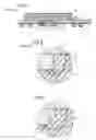
As illustrated in FIG. 1, an FBGA semiconductor component 1 contains a substrate 2. A semiconductor chip 4 is mounted on the chip side 3. The substrate 2 is provided with solder balls 6 on a solder ball side 5. In order to prevent solder from flowing away from the solder balls 6, a soldering resist mask 7 is furthermore applied to the solder ball side 5.
The solder balls 6 are fixed on ball pads 8. The ball pads 8 are electrically conductively connected to bonding pads 10 on the solder ball side 5 via a conductor structure 9 (shown in FIG. 4). For connecting the semiconductor chip 4 to the conductor structure 9, the bonding pads 10 are connected to bonding pads 12 on the semiconductor chip via wire bridges 11. For mechanical stabilization and for protection, the FBGA semiconductor component 1 is provided with a housing part 13, which covers the semiconductor chip 4, and with a housing part 14, which fills the bonding channel 15.
As illustrated in FIG. 1, the bonding channel 15, through which the wire bridges 11 are drawn, has smooth sidewalls 16. By virtue of this mechanical configuration, the housing part 14 is connected to the substrate 2 only in materially cohesive fashion. However, there is a positive locking joint between the housing part 14 and the wire bridge 11 since the housing part 14 encapsulates the wire bridge 11. On account of this inadequate connection between the housing part 14 and the substrate 2, a fracture 17 very often occurs in the housing part 14, as illustrated in FIG. 2. This fracture 17 runs over the wire bridge 11, which regularly leads to a fracture of the wire of the wire bridge 11.
A positively locking connection between the housing part 14 and the substrate 2 provides a remedy here. This is realized in a first exemplary embodiment in accordance with FIGS. 3 and 4 by virtue of the fact that a groove 18 running around the bonding channel 15 is introduced on the solder ball side 5, the groove being embodied in dovetailed fashion in cross section. In this dovetailed groove 18, during the shaping of the housing part 14, potting material can then pour into the groove 18 and the potting material in the groove then produces a positively locking connection between the substrate 2 and the housing part 14, thereby effectively avoiding a fracture 17 of the kind illustrated in FIG. 2.
FIG. 5 shows another configuration of the sidewall 16 of the bonding channel 15 in an undercut. In this case, the solder ball side 5 forms an angle α of less than 90° with the sidewall 16. The sidewall 16 correspondingly forms an angle β of less than 90° with the chip side 3. Accordingly, on the chip side 3 a larger space exists for the potting material of the housing part 14, as a result of which the housing part 14 is held in positively locking fashion in the substrate 2.
A further possibility for producing a positively locking joint between the housing part 14 and the substrate 2 consists in introducing a groove 19 into the sidewall 16, which groove, as illustrated in FIG. 6, is formed in T-shaped fashion. Potting material is introduced into this groove 19, too, during the production of the housing part 14, and it then provides for the positively locking connection.
A further possibility for realizing a positively locking joint between the housing part 14 and the substrate 2 consists, in accordance with FIG. 7, in providing the sidewall 16 with an unevenness 20. This can be done in an extremely simple manner by a procedure in which, when the bonding channel 15 is stamped out, the resulting roughness of the sidewalls 16 is not eliminated. This saves a technological step, on the one hand, and considerably improves the positively locking joinability, on the other hand.
A further possibility for producing a positively locking joint and stabilizing the bonding channel 15 is illustrated in FIGS. 8 and 9, in which a web 21 is introduced between the two sides in the longitudinal extent of the bonding channel 15, the web being mechanically fixedly connected to the sidewalls 16. As can be seen, the web 21 extends over the height of the bonding channel 15, that is to say between the chip side 3 and the solder ball side 5. The web 21 is expediently arranged such that it lies between the wire bridges 11 and, consequently, does not impede the bonding operation, that is to say the production of the wire bridges between the bonding pads 10 and 12.
Claims
What is claimed is:1. A semiconductor component comprising:
a substrate having a chip side, a solder ball side, and a bonding channel;
a semiconductor chip mounted on the chip side of the substrate;
a plurality of solder ball pads disposed on the solder ball side of the substrate;
a plurality of electrical connections extending through the bonding channel and electrically connected between the semiconductor chip and the solder ball pads; and
an encapsulation material covering the electrical connections within the bonding channel, wherein the encapsulation material extends within a surface of the substrate.
2. The semiconductor component according to claim 1, wherein the surface of the substrate includes a plurality of depressions on the solder ball side adjacent the bonding channel, the encapsulation material extending within the depressions.
3. The semiconductor component according to claim 2, wherein the depressions comprise grooves running around the bonding channel.
4. The semiconductor component according to claim 3, wherein the grooves have a T-shaped or dovetailed cross section.
5. The semiconductor component according to claim 1, wherein encapsulation material extends within a surface of the substrate along edges of the bonding channel.
6. The semiconductor component according to claim 5, wherein the edges of the bonding channel include an undercut such that edges of the bonding channel form an angle of less than 90° with the solder ball side of the substrate.
7. The semiconductor component according to claim 5, wherein the edges of the bonding channel include a groove, the encapsulation material extending within the groove.
8. The semiconductor component according to claim 7, wherein the groove is T-shaped or dovetailed in cross section.
9. The semiconductor component according to claim 5, wherein the edges of the bonding channel are uneven.
10. The semiconductor component comprising:
a substrate having a chip side, a solder ball side, and a bonding channel;
a semiconductor chip mounted on the chip side of the substrate;
a plurality of solder ball pads disposed on the solder ball side of the substrate;
a web arranged between a first sidewall of the bonding channel and a second sidewall of the bonding channel, the web attached to the substrate at each sidewall;
a plurality of electrical connections extending through the bonding channel and electrically connected between the semiconductor chip and the solder ball pads; and
an encapsulation material covering the electrical connections within the bonding channel.
11. A semiconductor component according to claim 10, wherein the web extends over the bonding channel on the solder ball side of the substrate.
12. The semiconductor component according to claim 10, wherein the web extends from one side of the bonding channel to an opposite side of the bonding channel and is in each case connected to the sidewalls.
13. The semiconductor component according to claim 12, wherein the web occupies the height of the bonding channel between the solder ball side and the chip side.
14. The semiconductor component according to claim 12, wherein the web only partly occupies the height of the bonding channel between the solder ball side and the chip side and is arranged near to the chip side.
15. The semiconductor component according to claim 10, wherein a plurality of webs are arranged over the bonding channel.
16. The semiconductor component according to claim 15, wherein the plurality of webs are arranged parallel to one another.
17. The semiconductor component of claim 10, wherein a surface of the substrate comprises at least one recess and the encapsulation material extends within the recess.
18. A substrate having a chip side for receiving a semiconductor chip, a solder ball side for applying solder balls on ball pads, and a bonding channel embodied as an opening between the chip side and the solder ball side and serving for leading through wire bridges between the semiconductor chip and bonding islands on the solder ball side, wherein said bonding channel has side areas extending between the chip side and the solder ball side and can be closed off with a housing part comprising potting composition, wherein the substrate includes at least one positively locking element for a potting composition that is arranged in that region of the substrate in which the housing part is produced.
19. The substrate according to claim 18, wherein the at least one positively locking element comprises a recess in a surface of the substrate.
20. The substrate according to claim 18, wherein the at least one positively locking element comprises a web that extends across the bonding channel.
Images & Drawings included:


Sources:
- United States Patent and Trademark Office - verify current appl. status at the USPTO↗
Recent applications in this class:
- » 20250273526 2025-08-28
FULLY MOLDED STRUCTURE WITH MULTI-HEIGHT COMPONENTS COMPRISING BACKSIDE CONDUCTIVE MATERIAL AND METHOD FOR MAKING THE SAME - » 20250266313 2025-08-21
SEMICONDUCTOR DEVICE PACKAGE AND METHOD OF MANUFACTURING THE SAME - » 20250233035 2025-07-17
SEMICONDUCTOR DEVICE AND METHOD OF MANUFACTURING A SEMICONDUCTOR DEVICE - » 20250210432 2025-06-26
ELECTRONIC PACKAGE AND MANUFACTURING METHOD THEREOF - » 20250201645 2025-06-19
FABRICATING PACKAGES WITH DUMMY DIES HAVING A CONSTRUCTION THAT MIMICS WARPAGE OF THE OTHER COMPONENTS INCLUDED IN THE PACKAGE - » 20250191990 2025-06-12
MANUFACTURING METHOD OF SEMICONDUCTOR PACKAGE - » 20250191989 2025-06-12
PACKAGE COMPRISING A SUBSTRATE WITH CAVITY AND AN INTEGRATED DEVICE WITH A STEP BACK SIDE - » 20250157870 2025-05-15
PACKAGE STRUCTURES - » 20250118609 2025-04-10
Semiconductor Packages and Methods of Forming - » 20250079248 2025-03-06
SEMICONDUCTOR PACKAGE AND METHOD OF MANUFACTURING SEMICONDUCTOR PACKAGE
Recent applications for this Assignee:
- » 20190222018 2019-07-18
Temperature sensing and fault detection for paralleled double-side cooled power modules - » 20190120879 2019-04-25
Readout circuit for resistive and capacitive sensors - » 20170125556 2017-05-04
Tunnel field effect transistors - » 20160072383 2016-03-10
System and method for a controlled feedback charge pump - » 20160064451 2016-03-03
Semiconductor component comprising magnetic field sensor - » 20150137309 2015-05-21
Methods of fabricating isolation regions of semiconductor devices and structures thereof - » 20120278520 2012-11-01
System and method of transmitting data between devices connected via a bus defining a time slot during transmission for responsive output information from bus devices - » 20120199909 2012-08-09
Semiconductor devices and methods of manufacture thereof - » 20120162924 2012-06-28
Integrated Semiconductor Outline Package - » 20120081105 2012-04-05
Signal generation for spectral measurements