Apparatus for solder crack deflection
US20070170592A1
2007-07-26
11/717,902
2007-03-13
✅ Patent granted
US 7,923,125 B2
2011-04-12
-
-
Charles D Garber | Andre′ C Stevenson
2028-08-02
Abstract:
An apparatus that includes a first component defining an interior of the apparatus; a first solder composition exterior to the first component; a second solder composition exterior to the first solder composition and the first component; and a second component exterior to the second solder composition, the first solder composition, and the first component.
Inventors:
- Chung C. Key 2 🇲🇾 Kedah, Malaysia
- Mustapha Mohd. Faizul 2 🇲🇾 Kedah, Malaysia
- Tan Siew Sang 2 🇲🇾 Kedah, Malaysia
Assignee:
- INTEL CORPORATION 47,158 🇺🇸 Santa Clara, CA, United States
Interested in similar patents?
Get notified when new applications in this technology area are published.
Classification:
H05K3/3436 » CPC main
Apparatus or processes for manufacturing printed circuits; Assembling printed circuits with electric components, e.g. with resistor electrically connecting electric components or wires to printed circuits by soldering; Surface mounted components; Leadless components having an array of bottom contacts, e.g. pad grid array or ball grid array components
H01L24/11 » CPC further
Arrangements for connecting or disconnecting semiconductor or solid-state bodies; Methods or apparatus related thereto; Means for bonding being attached to, or being formed on, the surface to be connected, e.g. chip-to-package, die-attach, "first-level" interconnects; Manufacturing methods related thereto; Bump connectors ; Manufacturing methods related thereto Manufacturing methods
H01L24/13 » CPC further
Arrangements for connecting or disconnecting semiconductor or solid-state bodies; Methods or apparatus related thereto; Means for bonding being attached to, or being formed on, the surface to be connected, e.g. chip-to-package, die-attach, "first-level" interconnects; Manufacturing methods related thereto; Bump connectors ; Manufacturing methods related thereto; Structure, shape, material or disposition of the bump connectors prior to the connecting process of an individual bump connector
H01L2224/13099 » CPC further
Indexing scheme for arrangements for connecting or disconnecting semiconductor or solid-state bodies and methods related thereto as covered by; Means for bonding being attached to, or being formed on, the surface to be connected, e.g. chip-to-package, die-attach, "first-level" interconnects; Manufacturing methods related thereto; Bump connectors; Manufacturing methods related thereto; Structure, shape, material or disposition of the bump connectors prior to the connecting process of an individual bump connector; Core members of the bump connector Material
H01L2924/01006 » CPC further
Indexing scheme for arrangements or methods for connecting or disconnecting semiconductor or solid-state bodies as covered by; Chemical elements Carbon [C]
H01L2924/01029 » CPC further
Indexing scheme for arrangements or methods for connecting or disconnecting semiconductor or solid-state bodies as covered by; Chemical elements Copper [Cu]
H01L2924/0103 » CPC further
Indexing scheme for arrangements or methods for connecting or disconnecting semiconductor or solid-state bodies as covered by; Chemical elements Zinc [Zn]
H01L2924/01033 » CPC further
Indexing scheme for arrangements or methods for connecting or disconnecting semiconductor or solid-state bodies as covered by; Chemical elements Arsenic [As]
H01L2924/01047 » CPC further
Indexing scheme for arrangements or methods for connecting or disconnecting semiconductor or solid-state bodies as covered by; Chemical elements Silver [Ag]
H01L2924/01051 » CPC further
Indexing scheme for arrangements or methods for connecting or disconnecting semiconductor or solid-state bodies as covered by; Chemical elements Antimony [Sb]
H01L2924/01075 » CPC further
Indexing scheme for arrangements or methods for connecting or disconnecting semiconductor or solid-state bodies as covered by; Chemical elements Rhenium [Re]
H01L2924/01082 » CPC further
Indexing scheme for arrangements or methods for connecting or disconnecting semiconductor or solid-state bodies as covered by; Chemical elements Lead [Pb]
H01L2924/01087 » CPC further
Indexing scheme for arrangements or methods for connecting or disconnecting semiconductor or solid-state bodies as covered by; Chemical elements Francium [Fr]
H01L2924/01322 » CPC further
Indexing scheme for arrangements or methods for connecting or disconnecting semiconductor or solid-state bodies as covered by; Alloys; Binary Alloys Eutectic Alloys, i.e. obtained by a liquid transforming into two solid phases
H01L2924/14 » CPC further
Indexing scheme for arrangements or methods for connecting or disconnecting semiconductor or solid-state bodies as covered by; Details of semiconductor or other solid state devices to be connected; Device type Integrated circuits
H01L2924/15311 » CPC further
Indexing scheme for arrangements or methods for connecting or disconnecting semiconductor or solid-state bodies as covered by; Details of package parts other than the semiconductor or other solid state devices to be connected; Die mounting substrate; Connection portion the connection portion being formed only on the surface of the substrate opposite to the die mounting surface being a ball array, e.g. BGA
H01L2924/15312 » CPC further
Indexing scheme for arrangements or methods for connecting or disconnecting semiconductor or solid-state bodies as covered by; Details of package parts other than the semiconductor or other solid state devices to be connected; Die mounting substrate; Connection portion the connection portion being formed only on the surface of the substrate opposite to the die mounting surface being a pin array, e.g. PGA
H05K3/3463 » CPC further
Apparatus or processes for manufacturing printed circuits; Assembling printed circuits with electric components, e.g. with resistor electrically connecting electric components or wires to printed circuits by soldering; Solder materials or compositions; Methods of application thereof Solder compositions in relation to features of the printed circuit board or the mounting process
H05K2201/10992 » CPC further
Indexing scheme relating to printed circuits covered by; Details of components or other objects attached to or integrated in a printed circuit board; Details of electrical connections of non-printed components, e.g. special leads; Other details of electrical connections Using different connection materials, e.g. different solders, for the same connection
Y02P70/50 » CPC further
Climate change mitigation technologies in the production process for final industrial or consumer products Manufacturing or production processes characterised by the final manufactured product
Y02P70/50 » CPC further
Climate change mitigation technologies in the production process for final industrial or consumer products Manufacturing or production processes characterised by the final manufactured product
Y10T428/12486 » CPC further
Stock material or miscellaneous articles; All metal or with adjacent metals Laterally noncoextensive components [e.g., embedded, etc.]
H01L2924/014 » CPC further
Indexing scheme for arrangements or methods for connecting or disconnecting semiconductor or solid-state bodies as covered by; Alloys Solder alloys
H01L2924/00013 » CPC further
Indexing scheme for arrangements or methods for connecting or disconnecting semiconductor or solid-state bodies as covered by; Technical content checked by a classifier Fully indexed content
H01L2224/29099 » CPC further
Indexing scheme for arrangements for connecting or disconnecting semiconductor or solid-state bodies and methods related thereto as covered by; Means for bonding being attached to, or being formed on, the surface to be connected, e.g. chip-to-package, die-attach, "first-level" interconnects; Manufacturing methods related thereto; Layer connectors, e.g. plate connectors, solder or adhesive layers; Manufacturing methods related thereto; Structure, shape, material or disposition of the layer connectors prior to the connecting process of an individual layer connector; Core members of the layer connector Material
H01L2924/15787 » CPC further
Indexing scheme for arrangements or methods for connecting or disconnecting semiconductor or solid-state bodies as covered by; Details of package parts other than the semiconductor or other solid state devices to be connected; Die mounting substrate; Material with a principal constituent of the material being a non metallic, non metalloid inorganic material Ceramics, e.g. crystalline carbides, nitrides or oxides
H01L2924/00 » CPC further
Indexing scheme for arrangements or methods for connecting or disconnecting semiconductor or solid-state bodies as covered by
H01L2924/00014 » CPC further
Indexing scheme for arrangements or methods for connecting or disconnecting semiconductor or solid-state bodies as covered by; Technical content checked by a classifier the subject-matter covered by the group, the symbol of which is combined with the symbol of this group, being disclosed without further technical details
H01L2224/0401 » CPC further
Indexing scheme for arrangements for connecting or disconnecting semiconductor or solid-state bodies and methods related thereto as covered by; Means for bonding being attached to, or being formed on, the surface to be connected, e.g. chip-to-package, die-attach, "first-level" interconnects; Manufacturing methods related thereto; Bonding areas; Manufacturing methods related thereto; Structure, shape, material or disposition of the bonding areas prior to the connecting process Bonding areas specifically adapted for bump connectors, e.g. under bump metallisation [UBM]
H01L23/48 IPC
Details of semiconductor or other solid state devices Arrangements for conducting electric current to or from the solid state body in operation, e.g. leads, terminal arrangements ; Selection of materials therefor
H01L21/44 IPC
Processes or apparatus adapted for the manufacture or treatment of semiconductor or solid state devices or of parts thereof; Manufacture or treatment of semiconductor devices or of parts thereof the devices having at least one potential-jump barrier or surface barrier, e.g. PN junction, depletion layer or carrier concentration layer the devices having semiconductor bodies not provided for in groups, , , and with or without impurities, e.g. doping materials Manufacture of electrodes on semiconductor bodies using processes or apparatus not provided for in groups -
Description
CROSS-REFERENCE TO RELATED APPLICATIONThis application is a divisional of U.S. patent application Ser. No. 10/306,946 filed Nov. 27, 2002.
BACKGROUND1. Field
The present invention relates generally to the bonding of components in an electronic system.
2. Description of Related Art
Microprocessors and many other complex electrical components may consist of a package that houses an integrated circuit (IC). The package, which acts as an electrical bridge between the IC and a printed circuit board, includes a substrate and an internal metallurgy system that routes power, ground, and signals between the printed circuit board and an IC attached to the substrate.
A package is typically connected to a printed circuit board using either a set of input/output pins (e.g., a “pin grid array”) or solder balls (e.g., a “ball grid array”). In a pin grid array package, arrays of input/output pins are connected to the bottom surface of the package. During assembly of a printed circuit board, the pin grid array is mated to a complimentary socket on the printed circuit board. One advantage to using pin grid array packages is that the package can later be removed from the printed circuit board and replaced.
Two technologies for manufacturing pin grid array packages are commonly used in the semiconductor manufacturing industry. These technologies are surface mount technology and wire bond technology. Surface mount technology involves attaching pins to conductive pads on the bottom surface of a ceramic substrate, thus forming electrical connections with the internal package routing system.
Because organic packages cannot be heated to extremely high temperatures without becoming damaged, and because it is impractical to surface mount pins using commonly used tin-lead (Sn—Pb) solder, wire bond technology is generally used to create organic packages with pin grid arrays.
Wire bond packages are generally larger than the IC that a package houses, since the package must accommodate the peripheral, inserted pin grid array. In order to reduce the size of organic packages, “flip-chip” ball grid array packages may be used. A “flip-chip” is a chip in which power, ground, and signal leads are brought to pads anywhere on the top surface of the chip. Sn—Pb solder bumps are then printed onto the pads, and the chip is turned upside down, and aligned with pads on the top surface of the package.
On the bottom of the package, a ball grid array is provided in order to attach the package to the printed circuit board. The ball grid array generally consists of solder balls that are attached to pads on the bottom of the package. These pads are then aligned with matching pads on the printed circuit board, and the board is heated, causing the solder to melt and form contacts between the package pads and the board pads. Flip-chip ball grid array packages can be substantially smaller than wire bond packages.
Connections are made in electronic systems by flip chip ball grid arrays (BGA), and other BGA types, for example, Flip Chip BGA, Wire Bond Plastic BGA, Ceramic BGA, micro BGA, very fine BGA, T-BGA, Chip Scale Package, etc.
There is a need in the art for a strong, stable bond between components in an electronic system.
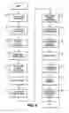
BRIEF DESCRIPTION OF THE DRAWINGSFIG. 1 illustrates a cross-sectional view of a pin grid array integrated circuit package;
FIG. 2 illustrates a side view of a flip-chip, ball grid array integrated circuit package;
FIG. 3 illustrates a side view of an integrated circuit package with a plurality of surface mount pins attached to a substrate;
FIG. 4 schematically illustrates a cross-sectional view of a first component having a first solder composition and a second solder composition on a surface thereof;
FIG. 5 schematically illustrates a cross-sectional view of a first component having a first solder composition and a second solder composition on a surface thereof connecting the first component to a second component;
FIG. 6 illustrates a flowchart of a method for attaching a second component to a first component for a first level interconnect;
FIG. 7 illustrates a general purpose computer system; and
FIG. 8 illustrates a flowchart of a method for attaching a second component to a first component for a second level interconnect.
The features of the described embodiments are specifically set forth in the appended claims. Referring to the following description and accompanying drawings, in which similar parts are identified by like reference numerals, best understand the embodiments.
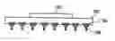
DETAILED DESCRIPTIONFIG. 1 illustrates a cross-sectional view of a ceramic, pin grid array integrated circuit package. Ceramic substrate 102 houses integrated circuit 104 on a top surface of the substrate. Attached to pin pads 106 on a bottom surface of substrate 102 are surface mount pins 108. During manufacture of the package, surface mount pins 108 may be brazed or soldered to substrate 102.
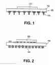
FIG. 2 illustrates a side view of a flip-chip ball grid array package. The package includes organic substrate 402 having array of solder balls 404 attached to a bottom surface of substrate 402. IC 406 is attached to a top surface of substrate 402 by solder bumps 408.
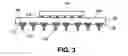
FIG. 3 illustrates a side view of an integrated circuit package with a plurality of surface mount pins attached to a substrate. The package includes substrate 502 (for example organic or non-organic) having top surface 504 and bottom surface 506. In one embodiment, substrate 502 could be any number of commonly used organic or inorganic materials, such as FR-5 or FR-4 epoxy-glass, polymide-glass, benzocyclobutene, Teflon, other epoxy resins, or the like in various embodiments. Typically, substrate 502 would have embedded therein a multilayer metallurgical system of interconnects (not shown), which electrically connect bonding pads on top surface 504 to pin pads 508 on bottom surface 506. FIG. 5 illustrates pin pads 508, but does not illustrate the interconnection between pads.
On bottom surface 506, surface mount pins 510 are attached to pin pads 508 on substrate 502, for example by brazing or soldering. In one embodiment, pins 510 are butt-head pins having a flattop head 512 and a post 514. In one embodiment, the diameter of pinhead 512 may be less than the diameter of pin pad 508. The dimensions of pad 508 and pinhead 512 can be chosen to best suit the particular application. In one embodiment, the outer edge of pinhead 512 is displaced inwardly from the outer edge of pad 508 by at least 0.005 inch, and in another embodiment, in the range of 0.015 to 0.025 inch. However, displacements greater or less than this range could also be used in other embodiments.
In one embodiment, pins 510 may be soldered to the central portions of pads 508.
IC 516 is electrically and mechanically connected to top surface 504 of substrate 502 via solder bumps 518. During the assembly process, pads on IC 516 and substrate 504 are aligned, and the solder bumps are heated to a temperature sufficient to melt the solder. The solder then flows onto adjoining pads (not shown) on top surface 504 of substrate 502. When cooled, IC 516 is firmly attached to substrate 502.
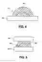
Referring now to FIG. 4, first component 400 has first solder material 402, and second solder material 404 surrounding first solder material 402. In one embodiment, first component 400 defines an interior of an assembly, with first solder material 402 exterior to first component 400, and second solder material 404 exterior to first solder material 402 and first component 400. First component 400 may be, for example, a conductive pad on an IC or package substrate.
Referring now to FIG. 5, there is illustrated a connection between two components. First component 500 is shown with first solder material 502 connected to first component 500. Second solder material 504 surrounds first solder material 502. Second component 506 is adjacent to second solder material 504. Second solder material 504 may also be connected to first component 500. First component 500 and second component may be, for example, a conductive pad.
In one embodiment, first component 500 defines an interior of an assembly. First solder material 502 is exterior to first component 500. Second solder material 504 is exterior to first solder material 502 and first component 500. Second component 506 is exterior to second solder material 504, first solder material 502, and first component 500.
In one embodiment, other solder materials and/or other components can be located between or adjacent to one or more of first component 500, first solder material 502, second solder material 504, and/or second component 506.
In one embodiment, first solder material 402 and/or 502 is stronger than second solder material 404 and/or 504. In another embodiment, first solder material 402 and/or 502 has a higher melting point than second solder material 404 and/or 504. In another embodiment, first solder material 402 and/or 502 has a higher shear strength than second solder material 404 and/or 504. In another embodiment, first solder material 402 and/or 502 has a higher tensile strength than second solder material 404 and/or 504.
In one embodiment, a solder's melting temperature depends on the composition of the solder.
In one embodiment, the first solder composition is a Sn—Sb composition with about 5 percent Sb by weight, with a melting temperature of about 240 degrees Celsius, while the second solder composition is a Sn—Sb composition with less than about 5 percent Sb by weight. Generally, if the composition includes a higher percentage of Sb, the melting temperature will be higher, and if the composition includes a lower percentage of Sb, the melting temperature will be lower.
In one embodiment, the first solder composition is a Sn—Sb composition with the amount of Sb in the range of about 4 to about 10 percent by weight. This composition has been shown to have a melting temperature that is higher than the melting temperature of the second solder composition which is a Sn—Pb solder.
In one embodiment the first solder composition contains about 5 percent Sb by weight. This composition has a melting temperature of about 240 degrees Celsius. In one embodiment, the second solder composition has a melting temperature of about 230 degrees Celsius for a Sn—Pb composition having 95 percent Sn by weight. The first and/or second compositions may include other elements as well.
In one embodiment, the second solder composition is a tin-lead (Sn—Pb) solder composition. Using a composition that includes from 60 to 95 percent Sn by weight, the melting temperature of Sn—Pb solder is within a range of 190 to 230 degrees Celsius. In one embodiment, the first solder composition is a tin-antimony (Sn—Sb) solder composition, which has a melting temperature that is higher than the melting temperature of most Sn—Pb solder compositions. In one embodiment, the melting temperature of the Sn—Sb solder composition is approximately 240 degrees Celsius, well above the melting temperature of Sn—Pb solder.
In another embodiment, for a lead free system, the first and/or second solder compositions could be selected from a group comprising tin/antimony (with tin being between about 55 to about 95 weight percent), tin/silver, tin/silver/copper (with silver and copper being between about 0.5 to about 3.0 weight percent), tin/silver/bismuth (with silver being between about 2.0 to about 4.5 weight percent and bismuth being between about 3.5 to about 7.5 weight percent), tin/silver/copper (with silver being between about 2.0 to about 4.5 weight percent and copper being between about 0.5 to about 3.0 weight percent), to name a few.
In another embodiment, for a lead free system, the first and/or second solder compositions could be selected from a group comprising tin/antimony (with tin being between about 55 to about 95 weight percent), tin/silver, tin/silver/copper (with silver and copper being between about 0.5 to about 3.0 weight percent), tin/silver/bismuth (with silver being between about 2.0 to about 4.5 weight percent and bismuth being between about 3.5 to about 7.5 weight percent), tin/silver/copper (with silver being between about 2.0 to about 4.5 weight percent and copper being between about 0.5 to about 3.0 weight percent), tin /zinc (with tin being about 91 weight percent), tin/bismuth (with tin being about 42 weight percent), to name a few.
In one embodiment, the first solder composition is 95/5 Sn/Sb or Sn/Ag (with Ag in the range of between about 3 to about 5 weight percent), which melts in the range of between about 220.degree. C. to about 240.degree. C.
In one embodiment, the second solder composition is 48/52 Sn/In or 43/57 Sn/Bi, which melts in the range of between about 120.degree. C. to about 140.degree. C.
In one embodiment, the second solder composition is Pb—Sn eutectic solder of 63 Sn/37 Pb which has a moderate melting temperature, particularly about 183 degree. C.
In another embodiment, the first and/or second solder compositions could be selected from solder alloys that include about 76 to 96 weight % Sn, about 0.2 to 2.5 weight % Cu, about 2 to 4.5 weight % Ag, about 0 to 12 weight % In, about 0 to 5.0 weight % Bi and about 0 to 2 weight % Sb. In one embodiment, the composition will include at least about 2.0 weight % In. In another embodiment, the composition will include at least 0.5 weight % Bi. In another embodiment, the composition will include greater than about 0 weight % Sb. In another embodiment, greater than about 0.01 weight % Sb.
In another embodiment, the first and/or second solder compositions could be selected from solder alloys that include about 81 to 93% Sn, about 0.2 to 1.0% Cu, about 2.5 to 4.5% Ag, and about 6 to 12% In. Unless otherwise identified in the descriptions and claims, all parts and percentages are by weight.
In one embodiment, Cu and Ag combined in proper dosages increase the fatigue resistance and lower the melting temperature of solder alloys. In one embodiment, the second solder composition includes at least about 0.5% Cu, and the first solder composition includes less than about 0.5% Cu.
In one embodiment, the second solder composition includes at least about 3.0% Ag, and the first solder composition includes less than about 3.0% Ag.
In one embodiment, the second solder composition includes at least about 3.0% to about 12.0% In, and the first solder composition includes from about 0% to about 9.0% In. In another embodiment, the first solder composition includes at least about 3.0% less In than the second solder composition.
In one embodiment, the first and/or second solder compositions includes at least about 0% to about 5.0% Bi.
In one embodiment, the first solder composition includes at least about 2.0% to about 10.0% Sb, and the second solder composition includes from about 0% to about 8.0% Sb. In another embodiment, the second solder composition includes at least about 2.0% less Sb than the first solder composition.
In one embodiment, the second solder composition is a 63 Sn/37 Pb solder with a melting temperature of about 183.degree. C. In another embodiment, the first solder composition is a 99.3 Sn 0.7 Cu solder with a melting temperature of about 227.degree. C. In another embodiment, the first solder composition is a 96.5 Sn 3.5 Ag solder with a melting temperature of about 227.degree. C.
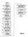
FIG. 6 illustrates a flowchart of a method for attaching a first component to a second component, for example for a first level interconnects. The method begins, in block 702, by providing a first component. In one embodiment, the first component is an organic substrate having a multi-level metallurgical system of interconnects and pads. In other embodiments, the first component can have only a single level of metallurgical connections, or can be an inorganic substrate.
In block 706, a first solder screen is placed over the first component. Generally, the first solder screen is a metal pattern (e.g., stainless steel) having holes that line up with desired solder locations on the first component. A first solder paste is applied over the first solder screen in block 708. A squeegee process is then performed, to deposit the first solder paste into the holes in the first solder screen, and thus desired solder locations on the first component. The amount of solder deposited in each hole is a function of the size of the holes and the thicknesses of the first solder screen and the desired thickness of the solder on the first component. Thus, the dimensions of the holes and the thicknesses of the first solder screen are selected based on the particular application. As will be explained below, the amount of solder deposited in each hole may affect the strength of the connection.
In block 710, the first solder screen is removed. The assembly is then heated, in block 712, to a temperature sufficient to reflow the solder. As discussed previously, the first solder composition may have a melting temperature that is higher than a melting temperature of solder used elsewhere in the component. However, the melting temperature of the first solder may be lower than a temperature that would damage the first component.
In block 714, the assembly is cooled in a controlled manner, to allow the solder to solidify. If the first solder composition has a greater percentage of antimony (Sb) by weight, the cooling process may need to be more carefully controlled, in order to mitigate the possible effects of phase separation.
In block 716, a second solder screen is placed over the first component. Generally, the second solder screen is a metal pattern (e.g., stainless steel) having holes that line up with desired solder locations on the first component. A second solder paste is applied over the solder screen in block 718. A squeegee process is then performed, to deposit the second solder paste into the holes in the second solder screen, and thus desired solder locations on the first component. The amount of solder deposited in each hole is a function of the size of the holes and the thicknesses of the second solder screen and the desired thickness of the solder on the first component. Thus, the dimensions of the holes and the thicknesses of the second solder screen are selected based on the particular application. As will be explained below, the amount of solder deposited in each hole may affect the strength of the connection.
In block 720, the second solder screen is removed. The assembly is then heated, in block 722, to a temperature sufficient to reflow the second solder composition.
In block 724, the assembly is cooled in a controlled manner, to allow the solder to solidify.
Once the first and second solder compositions are solidified, the package can be re-heated to melting temperature of second solder composition to attach the second component, in block 726, for example, using a solder reflow process.
Once the second component is attached, the assembly can be completed, in block 728. Completing the assembly typically involves hermetically sealing the assembly in order to protect the first and/or second components. The completed assembly can then be incorporated into a computer system in block 730, and the method ends.
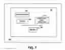
FIG. 7 illustrates a general-purpose computer system. Computer system 900 is housed on PC board 902, and includes bus 908, microprocessor 904, package 906, power supply signal generator 910, and memory 912. Package 906 includes surface mount pins that enable microprocessor 904 to be coupled to bus 908 through a socket on the PC board 902. The coupling of microprocessor 904 to bus 908 via package 906 enables power supply signals and non-power supply signals to be communicated between microprocessor 904 and devices coupled to bus 908. In one embodiment, bus 908 couples microprocessor 904 to memory 912 and power supply signal generator 910. However, it is to be understood that in alternative embodiments of the present invention, microprocessor 904 can be coupled to memory 912 and power supply signal generator 910 through two different busses. In addition, in alternative embodiments of the present invention, power supply signal generator 910 is not positioned on PC board 902, but instead is positioned elsewhere.
FIG. 8 illustrates a flowchart of a method for attaching a first component to a second component, for example for a second level interconnects. The method begins, in block 802, by providing a first component. In one embodiment, the first component is an organic substrate having a multi-level metallurgical system of interconnects and pads. In other embodiments, the first component can have only a single level of metallurgical connections, or can be an inorganic substrate.
In block 806, a first solder screen is placed over the first component. Generally, the first solder screen is a metal pattern (e.g., stainless steel) having holes that line up with desired solder locations on the first component. A first solder paste is applied over the first solder screen in block 808. A squeegee process is then performed, to deposit the first solder paste into the holes in the first solder screen, and thus desired solder locations on the first component. The amount of solder deposited in each hole is a function of the size of the holes and the thickness of the first solder screen and the desired thickness of the solder on the first component. Thus, the dimensions of the holes and the thickness of the first solder screen are selected based on the particular application. As will be explained below, the amount of solder deposited in each hole may affect the strength of the connection.
In block 810, the first solder screen is removed. The assembly is then heated, in block 812, to a temperature sufficient to reflow the solder. As discussed previously, the first solder composition may have a melting temperature that is higher than a melting temperature of solder used elsewhere in the component. However, the melting temperature of the first solder may be lower than a temperature that would damage the first component.
In block 814, the assembly is cooled in a controlled manner, to allow the solder to solidify. If the first solder composition has a greater percentage of antimony (Sb) by weight, the cooling process may need to be more carefully controlled, in order to mitigate the possible effects of phase separation.
In block 816, a second solder screen is placed over the first component. Generally, the second solder screen is a metal pattern (e.g., stainless steel) having holes that line up with desired solder locations on the first component. A second solder paste is applied over the solder screen in block 818. A squeegee process is then performed, to deposit the second solder paste into the holes in the second solder screen, and thus desired solder locations on the first component. The amount of solder deposited in each hole is a function of the size of the holes and the thickness of the second solder screen and the desired thickness of the solder on the first component. Thus, the dimensions of the holes and the thickness of the second solder screen are selected based on the particular application. As will be explained below, the amount of solder deposited in each hole may affect the strength of the connection.
In block 820, the second solder screen is removed.
In block 826, the second component is attached. The assembly is heated in block 828 to a temperature sufficient to reflow the second solder composition. In block 830, the assembly is cooled in a controlled manner, to allow the solder to solidify.
The assembly can then be incorporated into a computer system in block 832, and the method ends.
In one embodiment there is disclosed an apparatus that includes a first component defining an interior of the apparatus; a first solder composition exterior to the first component; a second different solder composition exterior to the first solder composition and the first component; and a second component exterior to the second solder composition, the first solder composition, and the first component.
In another embodiment there is disclosed an apparatus wherein the first solder composition either tougher and/or stronger than the second solder composition.
In another embodiment there is disclosed an apparatus wherein the first solder composition has higher shear strength than the second solder composition.
In another embodiment there is disclosed an apparatus wherein the first solder composition has a higher melting point than the second solder composition.
In another embodiment there is disclosed an apparatus wherein the first solder composition defines a dome shape having a height of about 0.1× to about 0.2× of a height of solder bump 408, for example for a first level interconnect. In another embodiment there is disclosed an apparatus wherein the first solder composition defines a dome shape having a height of about 0.075× to about 0.3× of a height of solder bump 408, for example for a first level interconnect. In another embodiment there is disclosed an apparatus wherein the first solder composition defines a dome shape having a height of about 0.05× to about 0.4× of a height of solder bump 408, for example for a first level interconnect.
In another embodiment there is disclosed an apparatus wherein the first solder composition defines a dome shape having a height of about 0.1× to about 0.2× of a diameter of solder ball 404, for example for a second level interconnect. In another embodiment there is disclosed an apparatus wherein the first solder composition defines a dome shape having a height of about 0.075× to about 0.3× of a diameter of solder ball 404, for example for a second level interconnect. In another embodiment there is disclosed an apparatus wherein the first solder composition defines a dome shape having a height of about 0.05× to about 0.4× of a diameter of solder ball 404, for example for a second level interconnect.
In another embodiment there is disclosed an apparatus wherein the first solder composition comprises tin, silver, copper, and less than about 0.5% antimony.
In another embodiment there is disclosed an apparatus that includes a first component; a first solder composition attached to a surface of the first component; a second different solder composition adjacent to, overlaying, and completely enclosing the first solder composition, wherein the second solder composition is attached to the first solder composition and the first component; and a second component attached to the second solder composition, wherein the first and second solder compositions form a laminate connection structure between the first component and the second component.
In another embodiment there is disclosed a method that includes depositing a first solder composition on a first component; depositing a second different solder composition on the first composition; attaching a second component to the second solder composition to form a connection between the first component and the second component.
In another embodiment there is disclosed a method or technique to be used for a Flip Chip Ball Grid Array (BGA) process. In another embodiment there is disclosed a method or technique for all second level of interconnect (package to board) on BGA interconnect type, for example, Flip Chip BGA, Wire Bond Plastic BGA, Ceramic BGA, micro BGA, very fine BGA, T-BGA, Chip Scale Package, etc.
In the preceding detailed description, specific embodiments were described. It will, however, be evident that various modifications and changes may be made thereto without departing from the broader spirit and scope as set forth in the claims. The specification and drawings are, accordingly, to be regarded in an illustrative rather than a restrictive sense.
Claims
1. An apparatus comprising:
a first component defining an interior of the apparatus;
a first solder composition exterior to the first component;
a second different solder composition exterior to the first solder composition and the first component; and
a second component exterior to the second solder composition, the first solder composition, and the first component.
2. The apparatus of claim 1, wherein the first solder composition is at least one of tougher and stronger than the second solder composition.
3. The apparatus of claim 1, wherein the first solder composition has a higher shear strength than the second solder composition.
4. The apparatus of claim 1, wherein the first solder composition has a higher melting point than the second solder composition.
5. The apparatus of claim 1, wherein the first solder composition defines a dome shape having a height of about 3 to about 5 mils.
6. The apparatus of claim 1, wherein the first solder composition defines a dome shape having a height of about 0.1 to about 0.2 times a total height of the first solder composition and the second solder composition.
7. The apparatus of claim 1, wherein the first solder composition comprises tin, silver, copper, and less than about 0.5% antimony.
8. The apparatus of claim 1, wherein the first component comprises a surface defining the interior and the first solder composition is on the surface, and wherein the first solder composition has a higher melting point than the second solder composition.
9. The apparatus of claim 1, wherein the second solder composition is physically touching the first component and the second component.
10. The apparatus of claim 1, wherein the first solder composition is copper, stronger, and has a higher melting point than the second solder composition.
11. The apparatus of claim 1, wherein the first solder composition and the second solder composition comprise at least one of tin, silver, copper, antimony, bismuth, and zinc; and wherein the first solder composition has a melting temperature that is higher than a melting temperature of the second solder composition.
12. An apparatus comprising:
a first component;
a first solder composition attached to a surface of the first component;
a second different solder composition adjacent to, overlaying, and completely enclosing the first solder composition, wherein the second solder composition is attached to the first solder composition and the first component; and
a second component attached to the second solder composition, wherein the first and second solder compositions form a laminate connection structure between the first component and the second component.
13. The apparatus of claim 12, wherein the first solder composition is at least one of tougher and stronger than the second solder composition.
14. The apparatus of claim 12, wherein the first solder composition has a higher shear strength than the second solder composition.
15. The apparatus of claim 12, wherein the first solder composition has a higher melting point than the second solder composition.
16. The apparatus of claim 12, wherein the first solder composition defines a dome shape having a height of about 3 to about 5 mils.
17. The apparatus of claim 12, wherein the first solder composition defines a dome shape having a height of about 0.1 to about 0.2 times a total height of the first solder composition and the second solder composition.
18. The apparatus of claim 12, wherein the first solder composition comprises tin, silver, copper, and less than about 0.5% antimony.
19. The apparatus of claim 12, wherein the second solder composition is physically touching the first component and the second component.
20. The apparatus of claim 12, wherein the first solder composition has a higher melting point than the second solder composition.
Images & Drawings included:
Sources:
- United States Patent and Trademark Office - verify current appl. status at the USPTO↗
Recent applications in this class:
- » 20250120020 2025-04-10
SIGNAL TRACE TRANSITION FOR HIGH DATA RATE APPLICATIONS - » 20250081357 2025-03-06
INTERPOSER FOR TROUBLESHOOTING A BALL GRID ARRAY (BGA) DEVICE AND COUPLING THE BGA DEVICE TO A PRINTED CIRCUIT BOARD WITH LIMITED HEAT EXPOSURE - » 20250024608 2025-01-16
CIRCUIT STRUCTURE - » 20240414851 2024-12-12
PRINTED CIRCUIT BOARD FOR A REFLOW PROFILING PROCESS - » 20240324109 2024-09-26
SOLDER BARRIER CONTACT FOR AN INTEGRATED CIRCUIT - » 20240284603 2024-08-22
REMOVABLE LID FOR FLIP CHIP-BALL GRID ARRAY (FC-BGA) PACKAGES - » 20240244761 2024-07-18
PACKAGES WITH A SHORTEST DISTANCE BETWEEN PACKAGE CONNECTORS AND A SEATING PLANE OF AT LEAST 6 MILS - » 20230328895 2023-10-12
ELECTRONIC COMPONENT MOUNTING STRUCTURE AND METHOD FOR MANUFACTURING SAME - » 20230240020 2023-07-27
Integrated circuit device with edge bond dam - » 20230225060 2023-07-13
SOLDER PADS WITH CONCAVE EDGES FOR BALL GRID ARRAYS
Recent applications for this Assignee:
- » 20250294866 2025-09-18
GATE CUT CONFINED WITHIN GATE TRENCH - » 20250294846 2025-09-18
BACKSIDE CROSS-COUPLE INTERCONNECTS - » 20250294835 2025-09-18
ELONGATED VERTICAL STRUCTURES OF CHANNEL MATERIALS - » 20250294827 2025-09-18
CO-INTEGRATION OF GATE-ALL-AROUND DEVICES WITH DIFFERENT NUMBERS OF NANORIBBONS - » 20250294818 2025-09-18
TRANSISTOR DESIGNS FOR FLOATING BODY MEMORY - » 20250294781 2025-09-18
MAGNETIC CORE INDUCTORS ON PACKAGE SUBSTRATES - » 20250294777 2025-09-18
INTEGRATED CIRCUIT DEVICE WITH MEMORY ARRAY AND SHARED GAIN ELEMENT - » 20250293985 2025-09-18
RECEIVER-BASED PRECISION CONGESTION CONTROL - » 20250293860 2025-09-18
PRESERVATION OF CONFIDENTIALITY AND INTEGRITY OF MODELS DURING EXECUTION - » 20250293706 2025-09-18
LOW-RANK DECOMPOSITION-BASED HARDWARE COMPRESSION OF MATRICES AND TENSORS