MULTI-COMPONENT ELECTRONIC PACKAGE WITH PLANARIZED EMBEDDED-COMPONENTS SUBSTRATE
US20080123318A1
2008-05-29
11/557,864
2006-11-08
Abstract:
An electronic multi-component package is assembled by placing multiple electronic components within multiple openings of a package substrate, then depositing and curing adhesive filler in gaps between the components and the inner peripheries of the openings. Circuit features, including conductive interconnects, are formed by thin-film photolithography over both front and back surfaces of the package substrate. Preformed conductive vias through the package substrate provide electrical connection between circuit features on opposite substrate surfaces. Additional electronic components may be attached to conductive lands on at least one side of the package. The circuit features also include contact pads for external package connections, such as in a ball-grid-array or equivalent structure.
Assignee:
- ATMEL CORPORATION 1,235 🇺🇸 San Jose, CA, United States
Interested in similar patents?
Get notified when new applications in this technology area are published.
Classification:
H01L2924/00014 » CPC further
Indexing scheme for arrangements or methods for connecting or disconnecting semiconductor or solid-state bodies as covered by; Technical content checked by a classifier the subject-matter covered by the group, the symbol of which is combined with the symbol of this group, being disclosed without further technical details
H05K1/185 » CPC main
Printed circuits; Printed circuits structurally associated with non-printed electric components associated with components mounted in the printed circuit board, e.g. insert mounted components [IMC] Components encapsulated in the insulating substrate of the printed circuit or incorporated in internal layers of a multilayer circuit
H01L21/568 » CPC further
Processes or apparatus adapted for the manufacture or treatment of semiconductor or solid state devices or of parts thereof; Manufacture or treatment of semiconductor devices or of parts thereof the devices having at least one potential-jump barrier or surface barrier, e.g. PN junction, depletion layer or carrier concentration layer; Assembly of semiconductor devices using processes or apparatus not provided for in a single one of the subgroups - , e.g. sealing of a cap to a base of a container; Encapsulations, e.g. encapsulation layers, coatings Temporary substrate used as encapsulation process aid
H01L21/6835 » CPC further
Processes or apparatus adapted for the manufacture or treatment of semiconductor or solid state devices or of parts thereof; Apparatus specially adapted for handling semiconductor or electric solid state devices during manufacture or treatment thereof; Apparatus specially adapted for handling wafers during manufacture or treatment of semiconductor or electric solid state devices or components ; Apparatus not specifically provided for elsewhere for supporting or gripping using temporarily an auxiliary support
H01L23/5389 » CPC further
Details of semiconductor or other solid state devices; Arrangements for conducting electric current within the device in operation from one component to another, i.e. interconnections, e.g. wires, lead frames the interconnection structure between a plurality of semiconductor chips being formed on, or in, insulating substrates the chips being integrally enclosed by the interconnect and support structures
H01L24/19 » CPC further
Arrangements for connecting or disconnecting semiconductor or solid-state bodies; Methods or apparatus related thereto; Means for bonding being attached to, or being formed on, the surface to be connected, e.g. chip-to-package, die-attach, "first-level" interconnects; Manufacturing methods related thereto; High density interconnect [HDI] connectors; Manufacturing methods related thereto Manufacturing methods of high density interconnect preforms
H01L24/24 » CPC further
Arrangements for connecting or disconnecting semiconductor or solid-state bodies; Methods or apparatus related thereto; Means for bonding being attached to, or being formed on, the surface to be connected, e.g. chip-to-package, die-attach, "first-level" interconnects; Manufacturing methods related thereto; High density interconnect [HDI] connectors; Manufacturing methods related thereto; Structure, shape, material or disposition of the high density interconnect connectors after the connecting process of an individual high density interconnect connector
H01L24/82 » CPC further
Arrangements for connecting or disconnecting semiconductor or solid-state bodies; Methods or apparatus related thereto; Methods for connecting semiconductor or other solid state bodies using means for bonding being attached to, or being formed on, the surface to be connected by forming build-up interconnects at chip-level, e.g. for high density interconnects [HDI]
H01L24/96 » CPC further
Arrangements for connecting or disconnecting semiconductor or solid-state bodies; Methods or apparatus related thereto; Batch processes at chip-level, i.e. with connecting carried out on a plurality of singulated devices, i.e. on diced chips the devices being encapsulated in a common layer, e.g. neo-wafer or pseudo-wafer, said common layer being separable into individual assemblies after connecting
H01L24/97 » CPC further
Arrangements for connecting or disconnecting semiconductor or solid-state bodies; Methods or apparatus related thereto; Batch processes at chip-level, i.e. with connecting carried out on a plurality of singulated devices, i.e. on diced chips the devices being connected to a common substrate, e.g. interposer, said common substrate being separable into individual assemblies after connecting
H01L25/03 » CPC further
Assemblies consisting of a plurality of individual semiconductor or other solid state devices ; Multistep manufacturing processes thereof all the devices being of a type provided for in the same subgroup of groups - , e.g. assemblies of rectifier diodes
H01L25/16 » CPC further
Assemblies consisting of a plurality of individual semiconductor or other solid state devices ; Multistep manufacturing processes thereof the devices being of types provided for in two or more different main groups of - , e.g. forming hybrid circuits
H01L21/561 » CPC further
Processes or apparatus adapted for the manufacture or treatment of semiconductor or solid state devices or of parts thereof; Manufacture or treatment of semiconductor devices or of parts thereof the devices having at least one potential-jump barrier or surface barrier, e.g. PN junction, depletion layer or carrier concentration layer; Assembly of semiconductor devices using processes or apparatus not provided for in a single one of the subgroups - , e.g. sealing of a cap to a base of a container; Encapsulations, e.g. encapsulation layers, coatings Batch processing
H01L24/48 » CPC further
Arrangements for connecting or disconnecting semiconductor or solid-state bodies; Methods or apparatus related thereto; Means for bonding being attached to, or being formed on, the surface to be connected, e.g. chip-to-package, die-attach, "first-level" interconnects; Manufacturing methods related thereto; Wire connectors; Manufacturing methods related thereto; Structure, shape, material or disposition of the wire connectors after the connecting process of an individual wire connector
H01L25/0652 » CPC further
Assemblies consisting of a plurality of individual semiconductor or other solid state devices ; Multistep manufacturing processes thereof all the devices being of a type provided for in the same subgroup of groups - , e.g. assemblies of rectifier diodes the devices not having separate containers the devices being of a type provided for in group the devices being arranged next and on each other, i.e. mixed assemblies
H01L2224/0401 » CPC further
Indexing scheme for arrangements for connecting or disconnecting semiconductor or solid-state bodies and methods related thereto as covered by; Means for bonding being attached to, or being formed on, the surface to be connected, e.g. chip-to-package, die-attach, "first-level" interconnects; Manufacturing methods related thereto; Bonding areas; Manufacturing methods related thereto; Structure, shape, material or disposition of the bonding areas prior to the connecting process Bonding areas specifically adapted for bump connectors, e.g. under bump metallisation [UBM]
H01L2224/04105 » CPC further
Indexing scheme for arrangements for connecting or disconnecting semiconductor or solid-state bodies and methods related thereto as covered by; Means for bonding being attached to, or being formed on, the surface to be connected, e.g. chip-to-package, die-attach, "first-level" interconnects; Manufacturing methods related thereto; Bonding areas; Manufacturing methods related thereto; Structure, shape, material or disposition of the bonding areas prior to the connecting process Bonding areas formed on an encapsulation of the semiconductor or solid-state body, e.g. bonding areas on chip-scale packages
H01L2224/24011 » CPC further
Indexing scheme for arrangements for connecting or disconnecting semiconductor or solid-state bodies and methods related thereto as covered by; Means for bonding being attached to, or being formed on, the surface to be connected, e.g. chip-to-package, die-attach, "first-level" interconnects; Manufacturing methods related thereto; High density interconnect [HDI] connectors; Manufacturing methods related thereto; Structure, shape, material or disposition of the high density interconnect connectors after the connecting process of an individual high density interconnect connector; Structure Deposited, e.g. MCM-D type
H01L2224/2518 » CPC further
Indexing scheme for arrangements for connecting or disconnecting semiconductor or solid-state bodies and methods related thereto as covered by; Means for bonding being attached to, or being formed on, the surface to be connected, e.g. chip-to-package, die-attach, "first-level" interconnects; Manufacturing methods related thereto; High density interconnect [HDI] connectors; Manufacturing methods related thereto; Structure, shape, material or disposition of the high density interconnect connectors after the connecting process of a plurality of high density interconnect connectors; Disposition being disposed on at least two different sides of the body, e.g. dual array
H01L2224/73267 » CPC further
Indexing scheme for arrangements for connecting or disconnecting semiconductor or solid-state bodies and methods related thereto as covered by; Means for bonding being of different types provided for in two or more of groups; Location after the connecting process on different surfaces Layer and HDI connectors
H01L2924/01005 » CPC further
Indexing scheme for arrangements or methods for connecting or disconnecting semiconductor or solid-state bodies as covered by; Chemical elements Boron [B]
H01L2924/01006 » CPC further
Indexing scheme for arrangements or methods for connecting or disconnecting semiconductor or solid-state bodies as covered by; Chemical elements Carbon [C]
H01L2924/01013 » CPC further
Indexing scheme for arrangements or methods for connecting or disconnecting semiconductor or solid-state bodies as covered by; Chemical elements Aluminum [Al]
H01L2924/01023 » CPC further
Indexing scheme for arrangements or methods for connecting or disconnecting semiconductor or solid-state bodies as covered by; Chemical elements Vanadium [V]
H01L2924/01027 » CPC further
Indexing scheme for arrangements or methods for connecting or disconnecting semiconductor or solid-state bodies as covered by; Chemical elements Cobalt [Co]
H01L2924/01033 » CPC further
Indexing scheme for arrangements or methods for connecting or disconnecting semiconductor or solid-state bodies as covered by; Chemical elements Arsenic [As]
H01L2924/01058 » CPC further
Indexing scheme for arrangements or methods for connecting or disconnecting semiconductor or solid-state bodies as covered by; Chemical elements Cerium [Ce]
H01L2924/01076 » CPC further
Indexing scheme for arrangements or methods for connecting or disconnecting semiconductor or solid-state bodies as covered by; Chemical elements Osmium [Os]
H01L2924/01078 » CPC further
Indexing scheme for arrangements or methods for connecting or disconnecting semiconductor or solid-state bodies as covered by; Chemical elements Platinum [Pt]
H01L2924/01082 » CPC further
Indexing scheme for arrangements or methods for connecting or disconnecting semiconductor or solid-state bodies as covered by; Chemical elements Lead [Pb]
H01L2924/014 » CPC further
Indexing scheme for arrangements or methods for connecting or disconnecting semiconductor or solid-state bodies as covered by; Alloys Solder alloys
H01L2924/09701 » CPC further
Indexing scheme for arrangements or methods for connecting or disconnecting semiconductor or solid-state bodies as covered by with a principal constituent of the material being a combination of two or more materials provided in the groups - ; Glass-ceramics, e.g. devitrified glass Low temperature co-fired ceramic [LTCC]
H01L2924/14 » CPC further
Indexing scheme for arrangements or methods for connecting or disconnecting semiconductor or solid-state bodies as covered by; Details of semiconductor or other solid state devices to be connected; Device type Integrated circuits
H01L2924/19042 » CPC further
Indexing scheme for arrangements or methods for connecting or disconnecting semiconductor or solid-state bodies as covered by; Details of hybrid assemblies other than the semiconductor or other solid state devices to be connected; Structure; Component type being an inductor
H01L2924/181 » CPC further
Indexing scheme for arrangements or methods for connecting or disconnecting semiconductor or solid-state bodies as covered by; Details of package parts other than the semiconductor or other solid state devices to be connected Encapsulation
H01L2224/97 » CPC further
Indexing scheme for arrangements for connecting or disconnecting semiconductor or solid-state bodies and methods related thereto as covered by; Batch processes at chip-level, i.e. with connecting carried out on a plurality of singulated devices, i.e. on diced chips the devices being connected to a common substrate, e.g. interposer, said common substrate being separable into individual assemblies after connecting
H05K3/4602 » CPC further
Apparatus or processes for manufacturing printed circuits; Manufacturing multilayer circuits characterized by a special circuit board as base or central core whereon additional circuit layers are built or additional circuit boards are laminated
H05K3/4602 » CPC further
Apparatus or processes for manufacturing printed circuits; Manufacturing multilayer circuits characterized by a special circuit board as base or central core whereon additional circuit layers are built or additional circuit boards are laminated
H05K2203/0165 » CPC further
Indexing scheme relating to apparatus or processes for manufacturing printed circuits covered by; Tools for processing; Objects used during processing; Carriers and holders Holder for holding a Printed Circuit Board [PCB] during processing, e.g. during screen printing
H05K2203/0165 » CPC further
Indexing scheme relating to apparatus or processes for manufacturing printed circuits covered by; Tools for processing; Objects used during processing; Carriers and holders Holder for holding a Printed Circuit Board [PCB] during processing, e.g. during screen printing
H05K2203/085 » CPC further
Indexing scheme relating to apparatus or processes for manufacturing printed circuits covered by; Treatments involving gases Using vacuum or low pressure
H05K2203/085 » CPC further
Indexing scheme relating to apparatus or processes for manufacturing printed circuits covered by; Treatments involving gases Using vacuum or low pressure
H05K2203/1469 » CPC further
Indexing scheme relating to apparatus or processes for manufacturing printed circuits covered by; Related to the order of processing steps; Applying or finishing the circuit pattern after another process, e.g. after filling of vias with conductive paste, after making printed resistors Circuit made after mounting or encapsulation of the components
Y10T29/4913 » CPC further
Metal working; Method of mechanical manufacture; Electrical device making; Conductor or circuit manufacturing; On flat or curved insulated base, e.g., printed circuit, etc. Assembling to base an electrical component, e.g., capacitor, etc.
Y10T29/49133 » CPC further
Metal working; Method of mechanical manufacture; Electrical device making; Conductor or circuit manufacturing; On flat or curved insulated base, e.g., printed circuit, etc.; Assembling to base an electrical component, e.g., capacitor, etc. with component orienting
Y10T29/49165 » CPC further
Metal working; Method of mechanical manufacture; Electrical device making; Conductor or circuit manufacturing; On flat or curved insulated base, e.g., printed circuit, etc.; Manufacturing circuit on or in base by forming conductive walled aperture in base
Y10T29/53183 » CPC further
Metal working; Means to assemble or disassemble; Means to assemble electrical device; Means to fasten electrical component to wiring board, base, or substrate Multilead component
H01L2224/81 » CPC further
Indexing scheme for arrangements for connecting or disconnecting semiconductor or solid-state bodies and methods related thereto as covered by; Methods for connecting semiconductor or other solid state bodies using means for bonding being attached to, or being formed on, the surface to be connected using a bump connector
H01L2224/85 » CPC further
Indexing scheme for arrangements for connecting or disconnecting semiconductor or solid-state bodies and methods related thereto as covered by; Methods for connecting semiconductor or other solid state bodies using means for bonding being attached to, or being formed on, the surface to be connected using a wire connector
H01L2924/00012 » CPC further
Indexing scheme for arrangements or methods for connecting or disconnecting semiconductor or solid-state bodies as covered by; Technical content checked by a classifier Relevant to the scope of the group, the symbol of which is combined with the symbol of this group
H01L2224/45099 » CPC further
Indexing scheme for arrangements for connecting or disconnecting semiconductor or solid-state bodies and methods related thereto as covered by; Means for bonding being attached to, or being formed on, the surface to be connected, e.g. chip-to-package, die-attach, "first-level" interconnects; Manufacturing methods related thereto; Wire connectors; Manufacturing methods related thereto; Structure, shape, material or disposition of the wire connectors prior to the connecting process of an individual wire connector; Core members of the connector Material
H01L2924/207 » CPC further
Indexing scheme for arrangements or methods for connecting or disconnecting semiconductor or solid-state bodies as covered by; Parameters Diameter ranges
H05K7/02 IPC
Constructional details common to different types of electric apparatus Arrangements of circuit components or wiring on supporting structure
H05K7/02 IPC
Constructional details common to different types of electric apparatus Arrangements of circuit components or wiring on supporting structure
B23P19/04 IPC
Machines for simply fitting together or separating metal parts or objects, or metal and non-metal parts, whether or not involving some deformation ; Tools or devices therefor so far as not provided for in other classes for assembling or disassembling parts
H01L21/027 IPC
Processes or apparatus adapted for the manufacture or treatment of semiconductor or solid state devices or of parts thereof; Manufacture or treatment of semiconductor devices or of parts thereof Making masks on semiconductor bodies for further photolithographic processing not provided for in group or
Description
TECHNICAL FIELD
The present invention relates to integrated circuit (IC) chip packages and the mounting of one or more IC dice to a support substrate and/or frame together with associated circuit components and interconnects.
BACKGROUND ART
Multi-component electronic packages and system-in-package (SIP) packages that are employed in the electronics industry today all utilize substrates for device inter-connection and attachment. Typical organic substrate materials are epoxy-glass, polyimide, and fluoropolymer laminates. Typical inorganic substrate materials are ceramics, low-temperature co-fire ceramics (LTCC) and silicon. The interconnect circuitry and component attach features are fabricated onto the substrates prior to components assembly.
With the exception of a silicon substrate, which employs thin-film metal deposition processes for the circuitry fabrication to yield line geometries on the order of one micrometer, all of the other substrate materials yield line geometries that are 50 micrometers or larger. A silicon substrate can only be used in single-sided applications and is often fragile in the final package form. The larger line geometries of the other substrates necessitate a larger final package size. The resultant longer interconnect lengths can also compromise package performance. Package designs with smaller package footprints and lower profiles, along with higher performance and yields, are ever being sought in the electronics industry.
SUMMARY DISCLOSURE
The present invention is method of assembling a multi-component electronic package and the package so formed in which microelectronic integrated circuit (IC) dice and/or discrete active/passive components are embedded into a “windowed” substrate carrier, planarized on both top and bottom surfaces. Electrically conductive interconnects and dielectric layers are deposited, or otherwise formed, on the top and bottom surfaces to electrically connect the embedded components.
In particular, a package substrate is provided, having defined front and back surfaces, with conductive vias through the package substrate. Multiple openings in the package substrate are sized to receive electronic components. After securing the package substrate on a vacuum support, multiple electronic components are placed within those openings and secured in place by the vacuum support. Adhesive filler material is deposited within a gap between the components and the inner peripheries of the corresponding openings, and then the filler is cured so as to permanently secure the embedded electronic components within the package substrate.
Circuit features are then formed in one or more layers over both front and back surfaces of the package substrate, for example, by thin-film photolithography. Features on opposite surfaces are electrically connected to each other by means of the conductive vias through package substrate. The circuit features include conductive interconnects that are electrically connected to the multiple electronic components embedded within the substrate. Integrated passive features, such as inductors, can also be formed during the circuitry fabrication process. Additional electronic components can be attached to resulting structure, e.g., at metal lands. A land-grid array, ball-grid array or pin-grid array can be formed on a back surface of the package substrate.
Package components are thus assembled onto the substrate to form an extremely compact, highly integrated, multi-component package or system-in-package (SIP) that provides an extremely small footprint and low profile. The electrical performance of the package is improved due to the ability to place the IC dice and other components in close proximity. The thin-film conductive interconnects formed on the planarized surfaces allow a much finer line width and spacing geometry in comparison with even the most advanced printed circuit board technologies. It also allows precise, high Q, integrated passive inductors to be formed in close proximity to the IC dice. With the interconnect layers deposited directly above and below the IC dice, a more efficient use is made of the package's footprint area, resulting in a smaller package size. The standard die-attach, wire bond or flip-chip attach processes can be eliminated by using this embedded components method.
BRIEF DESCRIPTION OF THE DRAWINGS
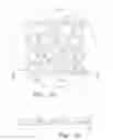
FIGS. 1A and 1B are respective top plan and side sectional views (the latter taken through the line 1B-1B in FIG. 1A) of a wafer substrate serving as a starting point for assembly of a multi-component electronic package in accord with the present invention.
FIGS. 2A through 2H are respective side sectional views, analogous to FIG. 1B, at various stages in a process of assembling an electronic package in accord with the present invention.
DETAILED DESCRIPTION
With reference to FIGS. 1A and 1B, a wafer 10 forms a substrate 12 for one or more IC chip packages. When cut into sections, e.g., 141, 142, 143, 144, each of those sections of the wafer 10 will define a separate package. The substrate 12 is typically composed of a dielectric material, such ceramics, glass, or plastics (e.g., epoxy, polyimide, or fluoropolymers). The substrate 12 has open cavities 16 into which IC die and other discrete electronic components will be placed. The width and length dimensions of the open cavities 16 are normally slightly larger than the components that will be inserted to allow tolerance for variations in the individual component size and room for adding an adhesive compound between the components and the inner periphery of the cavities 16.
Conductive vias 18 through the substrate 12 provide electrical pathways between the designated front and back surfaces 22F and 22B of the substrate 12 upon which electrical interconnects and other circuit elements (inductors, etc.) will be formed. Component lands 20, also conductive, may serve as attachment pads for discrete components, and also as land-grid, ball-grid or pin-grid pads for electrically connecting the resultant IC package to a printed circuit board or other system-level circuit structure.
With reference to FIG. 2A, a method of assembling the package begins with the aforementioned substrate 12 being mounted front-side down onto a die alignment vacuum plate 24. Various IC dice and discrete electrical components (active or passive) to be embedded in the substrate 12 are placed within the cavities 16. Preferably, IC dice will be place active side 32 down, so that the active side 32 will be generally coplanar with the front surface 22F of the substrate. In this way, we don't need to use a substrate having the same thickness as the IC dice, and the various IC dice being embedded need not all have the same thickness. Vacuum openings 26 in the vacuum plate 24 will hold the substrate 12, and the IC dice and other discrete components 30 in a fixed position.
With reference to FIG. 2B, normally the components 30 will be somewhat smaller in length and width dimensions than the cavities 16 in which they are place. The gaps between the components 30 and the inner peripheries of the cavities 16 are filled with an adhesive compound 34. After curing of the adhesive compound 34, the substrate 12 with its embedded components 30 is released by the vacuum plate 24. The cured adhesive compound 34 now holds the embedded components 30 in place. Depending on the adhesive compound being used to fill the gaps, the curing can be performed by application of heat (e.g., in a furnace) or by ultraviolet light. A self-curing adhesive (e.g., an epoxy resin with catalyst) could be also be used.
The designated back side of the package (opposite from that containing the active surfaces on the die) may be kept relatively planar by controlling the thicknesses of the die and discrete components, or may be made planar, if needed, by performing a post-embedding grind process, with a liquid dielectric coating added to facilitate the planarizing.
With reference to FIGS. 2D through 2F, thin-film deposition and photolithographic etching processes are used to build-up one or more layers circuit features over both surfaces 22B and 22F of the substrate assembly 12. On each side, there can be either a single layer of interconnects and other integrated circuit features, or, more usually, multiple layers of interconnects and features separated by dielectric material layers and connected where needed by vias.
For example, as seen in FIG. 2D, a thin-film metallic layer 38 may be deposited over the front surface 22F of the substrate assembly 12, followed by a photolithographic mask layer 40. After patterning and etching of the thin-film metallic layer 38, removal of the mask layer 40, and possible repeating of the deposition and patterning of additional layers, such as a dielectric layer, integrated circuit features result. These circuit features may include metal lands for and interconnects between the embedded IC dice and other embedded components 30, as well as integrated passive elements, such as thin-film inductors.
Likewise, further integrated circuit features are also formed on the back surface 22B, including metallic lands, by means of successive deposition, patterning and etching using one or more thin-film and mask layers 42 and 44, as seen in FIG. 2E.
The result is a substrate assembly 12 with patterned circuitry 38 and 42 on both front and back sides, 22F and 22B, of the substrate. As already noted with reference to FIGS. 1A and 1B, the circuitry on opposite sides of the substrate assembly 12 in FIG. 2F are connected to each other by means of the vias 18 that were pre-formed in the starting substrate.
With reference to FIG. 2G, additional electronic components can be attached to the resulting structure at metal lands on one of the surfaces, for example, above the front surface 22F. This may include die 50 attached with wire bonds 52, leaded packages 54 attached with their leads 56, ball-grid-array (BGA) packages 58 attached with solder balls 60, and discrete components 62. The opposite side of the assembly 12, for example, back side 22F, may have contact pads formed thereon, such as a BGA structure of solder balls 66. Alternatively, pins could be attached at metal lands on the back surface to form a pin-grid-array (PGA) package structure. Or, the lands themselves, formed on the back surface's thin film layer 42 in FIGS. 2E and 2F, could define a land-grid-array.
With reference to FIG. 2H, the electronic components 50, 54, 58, etc. above the front surface 22F may optionally be covered by an epoxy over-mold 70, coating or lid cover to protect them from damage during handling of the assembled package. Finally, the wafer 10 seen in FIG. 1A, now a completed package assembly, undergoes saw singulation into individual packages 74, 75, etc., with the cuts made along the dashed lines indicated in FIG. 1A that demarcate the various segments.
Claims
1. A method of assembling an multi-component electronic package, comprising:
providing a package substrate having defined front and back surfaces, with conductive vias through the package substrate providing electrical connections between the front and back surfaces, and with multiple openings in the package substrate adapted to receive electronic components;
securing the package substrate on a vacuum support;
placing multiple electronic components within the multiple openings of the package substrate, the electronic components being secured in place by the vacuum support, each electronic component being spaced from an inner periphery of its corresponding opening of the package substrate by a gap;
depositing an adhesive filler material within the gap and then curing the adhesive filler material, such that the electronic components within the openings are permanently secured to the package substrate; and
forming circuit features in one or more layers on both front and back surfaces of the package substrate, circuit features on opposite surfaces of the package substrate being electrically connected to each other by means of the conductive vias through the package substrate, the circuit features including conductive interconnects that are electrically connected to the multiple electronic components, the circuit features on at least one surface of the package substrate including a set of contact pads defining external connection locations for the assembled multi-component electronic package.
2. The method as in claim 1, wherein the package substrate comprises a dielectric material with metallic vias therethrough.
3. The method as in claim 1, wherein at least one of the multiple electronic components placed within the openings of the package substrate is an integrated circuit (IC) die.
4. The method as in claim 3, wherein the IC die has an active surface and the IC die is placed in an opening of the package substrate with its active surface coinciding with designated front surface of the package substrate.
5. The method as in claim 1, wherein the circuit features are formed by photolithography, with deposition a thin-film feature layer and a mask layer over the feature layer, patterning and etching of the feature layer using the mask layer, removal of the mask layer, and repeating to pattern additional feature layers.
6. The method as in claim 1, wherein the circuit features include integrated passive circuit elements.
7. The method as in claim 1, wherein the circuit features are successive formed first on one surface of the package substrate and then on the other surface of the package substrate.
8. The method as in claim 1, wherein the circuit features formed on the package substrate include conductive lands and the method further comprises attaching additional electronic components onto the designated front surface of the package substrate with electrical connections to the conductive lands.
9. The method as in claim 8, further comprising providing a protective covering over the additional electronic components.
10. The method as in claim 1, wherein the set of contact pads are formed as circuit features on a designated back surface of the package substrate.
11. The method as in claim 10, wherein the set of contact pads form a package contact structure selected from the group consisting of a land-grid-array, ball-grid-array and pin-grid-array.
12. The method as in claim 1, wherein the package substrate is a wafer for assembling multiple packages, and the method, after forming the circuit features, further includes segmenting the wafer into individual assembled packages.
13. A multi-component electronic package, comprising:
a package substrate having designated front and back surfaces with conductive vias through the substrate;
multiple electronic components embedded within the package substrate and secured thereto by a cured adhesive material; and
one or more layers of circuit features on both front and back surfaces of the package substrate, circuit features on opposite surfaces of the package substrate being electrically connected to each other by means of the conductive vias through the package substrate, the circuit features including conductive interconnects that are electrically connected to the multiple electronic components, the circuit features on at least one surface of the package substrate including a set of contact pads defining external connection locations for the electronic multi-component package.
14. The package as in claim 13, wherein the package substrate comprises a dielectric material with metallic vias therethrough.
15. The package as in claim 13, wherein at least one of the multiple electronic components embedded within the package substrate is an integrated circuit (IC) die.
16. The package as in claim 13, wherein the circuit features include integrated passive circuit elements.
17. The package as in claim 13, wherein the circuit features formed on the package substrate include conductive lands and the package further comprises additional electronic components attached to the designated front surface of the package substrate with electrical connections to the conductive lands.
18. The package as in claim 17, further comprising a protective covering over the additional electronic components.
19. The package as in claim 13, wherein the set of contact pads form a package contact structure selected from the group consisting of a land-grid-array, ball-grid-array and pin-grid-array.
Images & Drawings included:


Sources:
- United States Patent and Trademark Office - verify current appl. status at the USPTO↗
Recent applications in this class:
- » 20250168987 2025-05-22
MOLDED PACKAGES WITH THROUGH-MOLD INTERCONNECTS - » 20250126718 2025-04-17
PRINTED CIRCUIT BOARD - » 20250071906 2025-02-27
SUBSTRATE AND MODULE - » 20250063668 2025-02-20
Embedding Methods for Fine-Pitch Components and Corresponding Component Carriers - » 20250063667 2025-02-20
ELECTRONIC ASSEMBLY AND MANUFACTURING METHOD THEREOF - » 20250063666 2025-02-20
PRINTED CIRCUIT BOARD - » 20250056729 2025-02-13
SUBSTRATE - » 20250031312 2025-01-23
PRINTED CIRCUIT BOARD - » 20240381537 2024-11-14
Plateable Single Layer Capacitor - » 20240373559 2024-11-07
INTERFACE ASSEMBLY AND METHOD FOR MANUFACTURING INTERFACE ASSEMBLY
Recent applications for this Assignee:
- » 20190049494 2019-02-14
Microcontroller including power supply monitoring - » 20190026241 2019-01-24
Peripheral interface circuit for serial memory - » 20180253169 2018-09-06
Touch sensor with force sensor response normalization, and related method and apparatus - » 20180225452 2018-08-09
Input/output parameter selection - » 20180188699 2018-07-05
Autonomous process control peripheral - » 20180173669 2018-06-21
Serial device with configuration mode for changing device behavior - » 20180173657 2018-06-21
Automatic transmission of dummy bits in bus master - » 20180157443 2018-06-07
Microcontroller with integrated interface enabling reading data randomly from serial flash memory - » 20180089467 2018-03-29
Low cost cryptographic accelerator - » 20180068509 2018-03-08
Apparatus for locking and/or unlocking