Electronic part mounting board and method of mounting the same
US20080212301A1
2008-09-04
12/039,285
2008-02-28
✅ Patent granted
US 8,168,525 B2
2012-05-01
-
-
Hoa C Nguyen
2029-03-09
Abstract:
An electronic part mounting board includes an insulating board, a pad formed on the insulating board, a bump formed on the pad, and a film having heat resistance and electrical insulating properties and formed on the insulating board except the pad and the bump. A method of mounting an electronic part on the mounting board is also disclosed.
Assignee:
- NEC Corporation 20,055 🇯🇵 Tokyo, Japan
Interested in similar patents?
Get notified when new applications in this technology area are published.
Classification:
H01L2924/00014 » CPC further
Indexing scheme for arrangements or methods for connecting or disconnecting semiconductor or solid-state bodies as covered by; Technical content checked by a classifier the subject-matter covered by the group, the symbol of which is combined with the symbol of this group, being disclosed without further technical details
H01L2924/00011 » CPC further
Indexing scheme for arrangements or methods for connecting or disconnecting semiconductor or solid-state bodies as covered by; Technical content checked by a classifier Not relevant to the scope of the group, the symbol of which is combined with the symbol of this group
H05K3/3436 » CPC main
Apparatus or processes for manufacturing printed circuits; Assembling printed circuits with electric components, e.g. with resistor electrically connecting electric components or wires to printed circuits by soldering; Surface mounted components; Leadless components having an array of bottom contacts, e.g. pad grid array or ball grid array components
H01L24/81 » CPC further
Arrangements for connecting or disconnecting semiconductor or solid-state bodies; Methods or apparatus related thereto; Methods for connecting semiconductor or other solid state bodies using means for bonding being attached to, or being formed on, the surface to be connected using a bump connector
H05K3/303 » CPC further
Apparatus or processes for manufacturing printed circuits; Assembling printed circuits with electric components, e.g. with resistor Surface mounted components, e.g. affixing before soldering, aligning means, spacing means
H05K3/303 » CPC further
Apparatus or processes for manufacturing printed circuits; Assembling printed circuits with electric components, e.g. with resistor Surface mounted components, e.g. affixing before soldering, aligning means, spacing means
H05K3/3452 » CPC further
Apparatus or processes for manufacturing printed circuits; Assembling printed circuits with electric components, e.g. with resistor electrically connecting electric components or wires to printed circuits by soldering Solder masks
H05K3/3452 » CPC further
Apparatus or processes for manufacturing printed circuits; Assembling printed circuits with electric components, e.g. with resistor electrically connecting electric components or wires to printed circuits by soldering Solder masks
H01L24/16 » CPC further
Arrangements for connecting or disconnecting semiconductor or solid-state bodies; Methods or apparatus related thereto; Means for bonding being attached to, or being formed on, the surface to be connected, e.g. chip-to-package, die-attach, "first-level" interconnects; Manufacturing methods related thereto; Bump connectors ; Manufacturing methods related thereto; Structure, shape, material or disposition of the bump connectors after the connecting process of an individual bump connector
H01L2224/81001 » CPC further
Indexing scheme for arrangements for connecting or disconnecting semiconductor or solid-state bodies and methods related thereto as covered by; Methods for connecting semiconductor or other solid state bodies using means for bonding being attached to, or being formed on, the surface to be connected using a bump connector involving a temporary auxiliary member not forming part of the bonding apparatus
H01L2224/81192 » CPC further
Indexing scheme for arrangements for connecting or disconnecting semiconductor or solid-state bodies and methods related thereto as covered by; Methods for connecting semiconductor or other solid state bodies using means for bonding being attached to, or being formed on, the surface to be connected using a bump connector; Arrangement of the bump connectors prior to mounting wherein the bump connectors are disposed only on another item or body to be connected to the semiconductor or solid-state body
H01L2224/812 » CPC further
Indexing scheme for arrangements for connecting or disconnecting semiconductor or solid-state bodies and methods related thereto as covered by; Methods for connecting semiconductor or other solid state bodies using means for bonding being attached to, or being formed on, the surface to be connected using a bump connector Applying energy for connecting
H01L2224/81801 » CPC further
Indexing scheme for arrangements for connecting or disconnecting semiconductor or solid-state bodies and methods related thereto as covered by; Methods for connecting semiconductor or other solid state bodies using means for bonding being attached to, or being formed on, the surface to be connected using a bump connector; Bonding techniques Soldering or alloying
H01L2924/01005 » CPC further
Indexing scheme for arrangements or methods for connecting or disconnecting semiconductor or solid-state bodies as covered by; Chemical elements Boron [B]
H01L2924/01006 » CPC further
Indexing scheme for arrangements or methods for connecting or disconnecting semiconductor or solid-state bodies as covered by; Chemical elements Carbon [C]
H01L2924/01033 » CPC further
Indexing scheme for arrangements or methods for connecting or disconnecting semiconductor or solid-state bodies as covered by; Chemical elements Arsenic [As]
H01L2924/01082 » CPC further
Indexing scheme for arrangements or methods for connecting or disconnecting semiconductor or solid-state bodies as covered by; Chemical elements Lead [Pb]
H01L2924/014 » CPC further
Indexing scheme for arrangements or methods for connecting or disconnecting semiconductor or solid-state bodies as covered by; Alloys Solder alloys
H01L2924/14 » CPC further
Indexing scheme for arrangements or methods for connecting or disconnecting semiconductor or solid-state bodies as covered by; Details of semiconductor or other solid state devices to be connected; Device type Integrated circuits
H05K3/3457 » CPC further
Apparatus or processes for manufacturing printed circuits; Assembling printed circuits with electric components, e.g. with resistor electrically connecting electric components or wires to printed circuits by soldering Solder materials or compositions; Methods of application thereof
H05K3/3489 » CPC further
Apparatus or processes for manufacturing printed circuits; Assembling printed circuits with electric components, e.g. with resistor electrically connecting electric components or wires to printed circuits by soldering Composition of fluxes; Methods of application thereof; Other methods of activating the contact surfaces
H05K2201/09909 » CPC further
Indexing scheme relating to printed circuits covered by; Shape and layout; Shape or layout details not covered by a single group of - Special local insulating pattern, e.g. as dam around component
H05K2201/09909 » CPC further
Indexing scheme relating to printed circuits covered by; Shape and layout; Shape or layout details not covered by a single group of - Special local insulating pattern, e.g. as dam around component
H05K2201/2036 » CPC further
Indexing scheme relating to printed circuits covered by; Details of printed circuits not provided for in - Permanent spacer or stand-off in a printed circuit or printed circuit assembly
H05K2201/2036 » CPC further
Indexing scheme relating to printed circuits covered by; Details of printed circuits not provided for in - Permanent spacer or stand-off in a printed circuit or printed circuit assembly
H05K2203/0769 » CPC further
Indexing scheme relating to apparatus or processes for manufacturing printed circuits covered by; Treatments involving liquids, e.g. plating, rinsing; Uses of liquids, e.g. rinsing, coating, dissolving Dissolving insulating materials, e.g. coatings, not used for developing resist after exposure
Y02P70/50 » CPC further
Climate change mitigation technologies in the production process for final industrial or consumer products Manufacturing or production processes characterised by the final manufactured product
Y02P70/50 » CPC further
Climate change mitigation technologies in the production process for final industrial or consumer products Manufacturing or production processes characterised by the final manufactured product
Y10T29/4913 » CPC further
Metal working; Method of mechanical manufacture; Electrical device making; Conductor or circuit manufacturing; On flat or curved insulated base, e.g., printed circuit, etc. Assembling to base an electrical component, e.g., capacitor, etc.
Y10T29/49147 » CPC further
Metal working; Method of mechanical manufacture; Electrical device making; Conductor or circuit manufacturing; On flat or curved insulated base, e.g., printed circuit, etc. Assembling terminal to base
H01L2224/0401 » CPC further
Indexing scheme for arrangements for connecting or disconnecting semiconductor or solid-state bodies and methods related thereto as covered by; Means for bonding being attached to, or being formed on, the surface to be connected, e.g. chip-to-package, die-attach, "first-level" interconnects; Manufacturing methods related thereto; Bonding areas; Manufacturing methods related thereto; Structure, shape, material or disposition of the bonding areas prior to the connecting process Bonding areas specifically adapted for bump connectors, e.g. under bump metallisation [UBM]
H05K7/10 IPC
Constructional details common to different types of electric apparatus; Arrangements of circuit components or wiring on supporting structure Plug-in assemblages of components, e.g. IC sockets
H05K7/10 IPC
Constructional details common to different types of electric apparatus; Arrangements of circuit components or wiring on supporting structure Plug-in assemblages of components, e.g. IC sockets
H05K3/00 IPC
Apparatus or processes for manufacturing printed circuits
H05K3/00 IPC
Apparatus or processes for manufacturing printed circuits
H01L21/44 IPC
Processes or apparatus adapted for the manufacture or treatment of semiconductor or solid state devices or of parts thereof; Manufacture or treatment of semiconductor devices or of parts thereof the devices having at least one potential-jump barrier or surface barrier, e.g. PN junction, depletion layer or carrier concentration layer the devices having semiconductor bodies not provided for in groups, , , and with or without impurities, e.g. doping materials Manufacture of electrodes on semiconductor bodies using processes or apparatus not provided for in groups -
Description
This application is based upon and claims the benefit of priority from Japanese patent application No. 2007-051267, filed on Mar. 1, 2007, the disclosure of which is incorporated herein in its entirety by reference.
BACKGROUND OF THE INVENTION
The present invention relates to a board on which an electronic part is mounted and a method of mounting the same.
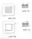
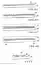
Conventionally, to mount a semiconductor chip (or a BOA (Ball Grid Array)) on a board, solder bumps 102 are respectively formed on pads 101 on a board 100, as shown in FIG. 4A. A flux 103 is applied to the board 100, as shown in FIG. 4B. A semiconductor chip (or BGA) 104 is mounted on the board 100, as shown in FIG. 4C. The semiconductor chip (or BOA) and the board 100 are soldered by a reflow, as shown in FIG. D.
Reference 1 (Japanese Patent Laid-Open No. 57-210638) discloses another conventional mounting method. As shown in FIG. 5, according to this mounting method, to perform soldering by a reflow, a frame-like flow preventing member (dam) 204 is formed to prevent solder bumps 202 from flowing outside corresponding pads 201. Referring to FIG. 5, reference numeral 200 denotes a board; and 203, a semiconductor chip.
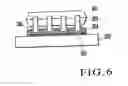
Reference 2 (Japanese Patent Laid-Open No. 7-015122) discloses still another conventional mounting method. As shown in FIG. 6, according to this mounting method, a cream solder is filled to form cream solder portions 305 in corresponding openings of a film having electrical insulation and heat resistance properties to prepare a bonding film assembly 304. The bonding film assembly 304 is fed onto a board 300 to overlap the cream solder portions 305 on corresponding pads 301 of the board 300. An electronic part 302 is fed onto the film assembly 304 to overlap leads 303 of the electronic part 302 onto the corresponding cream solder portions 305. The board 300 is heated to melt the cream solder portions 305. As described above, the film assembly 304 prevents the overflow of the cream solder portions 305.
According to the conventional mounting method shown in FIGS. 4A to 4D, a soldering failure such as a solder short 105 and a solder wetting failure 106 may occur in the step shown in FIG. 4D, thereby posing a problem.
The mounting method disclosed in reference 1 can prevent the solder bump flow outside the corresponding pad. However, like in FIGS. 4A to 4D, soldering failures cannot be prevented.
The mounting method disclosed in reference 2, to mount a bare chip with a small pitch, the paste flowing from the film shorts, resulting in a soldering failure.
SUMMARY OF THE INVENTION
The present invention has been made to solve the conventional problems described above and has as its object to reduce soldering failures.
According to an aspect of the present invention, there is provided an electronic part mounting board comprising an insulating board, a pad formed on the insulating board, a bump formed on the pad, and a film having heat resistance and electrical insulating properties and formed on the insulating board except the pad and the bump.
According to another aspect of the present invention, there is provided a method of mounting an electronic part, comprising the steps of preparing an electronic part mounting board, the mounting board including an insulating board, a pad formed on the insulating board, a bump formed on the pad, and a film having heat resistance and electrical insulating properties and formed on the insulating board except the pad and the bump, placing the electronic part on the mounting board so that an electrode of the electronic part overlaps the bump, and melting the solder bump to bond the pad and the electrode of the electronic part by solder.
BRIEF DESCRIPTION OF THE DRAWINGS
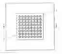
FIG. 1A is a plan view showing a mounting board according to an embodiment of the present invention;
FIG. 1B is a sectional view taken along the line I-I of the mounting board in FIG. 1A;
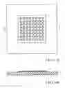
FIGS. 2A to 2C are plan views showing a method of manufacturing the mounting board shown in FIG. 1;
FIGS. 2D to 2F are enlarged sectional views of a portion indicated by a point a in each of FIGS. 2A to 2C;
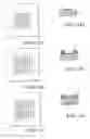
FIGS. 3A and 3B are plan views showing a method of mounting an electronic part on the mounting board shown in FIG. 1;
FIGS. 3C and 3D are enlarged sectional views showing a portion indicated by a point a in each of FIGS. 3A and 3B;
FIGS. 4A to 4D are sectional views showing a conventional mounting method of mounting a semiconductor chip or BGA on a board;
FIG. 5 is a sectional view of an integrated circuit showing another conventional mounting method; and
FIG. 6 is a sectional view of an integrated circuit showing still another conventional mounting method.
DESCRIPTION OF THE PREFERRED EMBODIMENT
An embodiment of the present invention will be described with reference to the accompanying drawings.
As shown in FIGS. 1A and 1B, a mounting board according to an embodiment of the present invention comprises an insulating board 1 on which an electronic part such as a semiconductor chip or BGA is mounted, pads 1 serving as conductive layers connected to the corresponding electrodes of the electronic part, bumps 3 respectively formed on the pads 2, and a film 4 having electrical insulating and heat resistance properties and formed on the insulating board 1.
This mounting board is characterized in that the film 4 is formed on the insulating board I except the bumps 3. The film 4 has the electrical insulating properties and heat resistance against the reflow temperature when mounting an electronic part. If the film 4 must be removed upon mounting the electronic part, a material such as a polyimide film soluble with an organic solvent can be used as the material of the film 4. The height of the film 4 is larger than that of each pad 2.
A method of manufacturing a mounting board and a method of mounting an electronic part on the mounting board according to this embodiment will be described below.
First of all, the method of manufacturing a mounting board will be described with reference to FIGS. 2A to 2F. As shown in FIGS. 28 and 2E, a film 4 is formed on an insulating substrate 1 shown in FIGS. 2A and 2D except pads 2. When the film is formed using soluble polyimide, for example, the polyimide is applied to the insulating board 1 and cured. The polyimide is patterned by etching to remove the polyimide corresponding to the pads 2.
Subsequently, as shown in FIGS. 2C and 2F, bumps 3 are respectively formed on the pads 2, thus finishing the mounting board shown in FIGS. 1A and 1B.
In the order opposite to that described above, the bumps 3 may be formed on the pads 3, respectively, and then the film 4 may be formed on the insulating board 1 except the pads 2 and the bumps 3.
The method of mounting an electronic part on the mounting board will be described with reference to FIGS. 3A to 3D. As shown in FIGS. 3A and 3C, a flux 5 is applied to a mounting board. Note that this step may be omitted.
Subsequently, an electronic part 6 such as a semiconductor chip or BGA is placed on the mounting board such that the electrodes of the electronic part 6 respectively overlap bumps 3. A load such as a counterweight is placed on the electronic part 6 to melt the solder bumps 3 by the reflow, thereby bonding the pads 2 and the corresponding electrodes of the electronic part 6 by the solder. As shown in FIGS. 3B and 3D, the electronic part 6 is completely mounted on the mounting board.
If the film 4 must be removed, the film 4 is removed with an organic solvent or the like after the steps in FIGS. 3B and 3D.
As described above, according to this embodiment, the film 4 is sandwiched between the electronic part 6 and the insulating board 1 to eliminate the shortage of the flux 5 during the reflow. The stand-off height between the electronic part 6 and the insulating board l can be ensured. Therefore, the reflow can be performed while applying the load on the electronic part 6. This makes it possible to prevent solder wetting failures and positional errors between the electronic part 6 and the insulating board 1.
According to this embodiment, since the adjacent bumps can be perfectly separated from each other by the film 4, the solder short can be prevented.
According to this embodiment, the stand-off height after the reflow can be controlled by the thickness of the film.
According to this embodiment, when the soluble film 4 is used, the film 4 can be removed by dissolution upon mounting the electronic part 6.
The present invention is applicable to mounting of an electronic part such as a semiconductor chip or BGA.
While the invention has been particularly shown and described with reference to exemplary embodiments thereof, the invention is not limited to these embodiments. It will be understood by those of ordinary skill in the art that various changes in form and details may be made therein without departing from the spirit and scope of the present invention as defined by the claims.
Claims
What is claimed is:1. An electronic part mounting board comprising:
an insulating board;
a pad formed on said insulating board;
a bump formed on said pad; and
a film having heat resistance and electrical insulating properties and formed on said insulating board except said pad and said bump.
2. A board according to claim 1, wherein said film comprises a soluble film.
3. A method of mounting an electronic part, comprising the steps of:
preparing an electronic part mounting board, the mounting board including an insulating board, a pad formed on the insulating board, a bump formed on the pad, and a film having heat resistance and electrical insulating properties and formed on the insulating board except the pad and the bump;
placing the electronic part on the mounting board so that an electrode of the electronic part overlaps the bump; and
melting the solder bump to bond the pad and the electrode of the electronic part by solder.
4. A method according to claim 3, wherein the preparing step comprises the steps of:
forming a film on the insulating board except the pad on the insulating board; and
forming a solder bump on the pad after forming the film.
5. A method according to claim 3, wherein the preparing step comprises the steps of:
forming the bump on the pad on the insulating board; and
forming a film on the insulating board except the pad and the bump after forming the bump.
6. A method according to claim 3, further comprising the step of removing the film after bonding, the film being soluble.
Images & Drawings included:
Sources:
- United States Patent and Trademark Office - verify current appl. status at the USPTO↗
Similar patent applications:
- » 20050230147
Wiring board, and electronic device with an electronic part mounted on a wiring board, as well as method of mounting an electronic part on a wiring board - » 10419197
Wiring board, and electronic device with an electronic part mounted on a wiring board, as well as method of mounting an electronic part on a wiring board - » 20050146019
Wiring board, and electronic device with an electronic part mounted on a wiring board, as well as method of mounting an electronic part on a wiring board - » 20070051778
Lead-type electronic-part-mounted printed circuit board, method of soldering lead-type electronic part and air-conditioner - » 20100193233
Dual inline lead-type electronic-part-mounted printed circuit board, method of soldering dual inline lead-type electronic part, printed circuit board and air-conditioner - » 10763495
Method for mounting electronic parts onto a board - » 10216126
Method for mounting electronic parts on a board - » 20150043125
Multilayer ceramic electronic part, board having the same mounted thereon, and manufacturing method thereof - » 10635314
Method of mounting electronic parts on a flexible printed circuit board - » 20080006296
Cleaning Device of Board and Cleaning Method, Flat Display Panel, Mounting Equipment of Electronic Parts and Mounting Method
Recent applications in this class:
- » 20250120020 2025-04-10
SIGNAL TRACE TRANSITION FOR HIGH DATA RATE APPLICATIONS - » 20250081357 2025-03-06
INTERPOSER FOR TROUBLESHOOTING A BALL GRID ARRAY (BGA) DEVICE AND COUPLING THE BGA DEVICE TO A PRINTED CIRCUIT BOARD WITH LIMITED HEAT EXPOSURE - » 20250024608 2025-01-16
CIRCUIT STRUCTURE - » 20240414851 2024-12-12
PRINTED CIRCUIT BOARD FOR A REFLOW PROFILING PROCESS - » 20240324109 2024-09-26
SOLDER BARRIER CONTACT FOR AN INTEGRATED CIRCUIT - » 20240284603 2024-08-22
REMOVABLE LID FOR FLIP CHIP-BALL GRID ARRAY (FC-BGA) PACKAGES - » 20240244761 2024-07-18
PACKAGES WITH A SHORTEST DISTANCE BETWEEN PACKAGE CONNECTORS AND A SEATING PLANE OF AT LEAST 6 MILS - » 20230328895 2023-10-12
ELECTRONIC COMPONENT MOUNTING STRUCTURE AND METHOD FOR MANUFACTURING SAME - » 20230240020 2023-07-27
Integrated circuit device with edge bond dam - » 20230225060 2023-07-13
SOLDER PADS WITH CONCAVE EDGES FOR BALL GRID ARRAYS
Recent applications for this Assignee:
- » 20250295043 2025-09-18
SUPERCONDUCTING QUANTUM CIRCUIT - » 20250294700 2025-09-18
ELECTRONIC DEVICE RACK, ELECTRONIC DEVICE UNIT, AND METHOD OF INSTALLING ELECTRONIC DEVICE RACK - » 20250294570 2025-09-18
RADIO ACCESS NETWORK NODE, RADIO TERMINAL, AND METHODS AND NON-TRANSITORY COMPUTER-READABLE MEDIA THEREFOR - » 20250294518 2025-09-18
MONITORING DEVICE, TRACKING METHOD, AND NON-TRANSITORY COMPUTER-READABLE MEDIUM - » 20250294486 2025-09-18
METHOD, DEVICE AND COMPUTER READABLE MEDIUM FOR COMMUNICATIONS - » 20250294444 2025-09-18
CELL SELECTION BASED ON USER CAPABILITY - » 20250293871 2025-09-18
PRIVATE KEY RECOVERY DEVICE, PRIVATE KEY RECOVERY METHOD, AND STORAGE MEDIUM - » 20250293866 2025-09-18
QUANTUM KEY DISTRIBUTION SYSTEM, KEY MANAGEMENT APPARATUS, AND KEY MANAGEMENT METHOD - » 20250293833 2025-09-18
METHODS, DEVICES, AND COMPUTER READABLE MEDIUM FOR COMMUNICATION - » 20250293791 2025-09-18
COMMUNICATION CONTROL APPARATUS, COMMUNICATION APPARATUS, COMMUNICATION SYSTEM, STORAGE MEDIUM, AND COMMUNICATION CONTROL METHOD