System-in-package packaging for minimizing bond wire contamination and yield loss
US20100164091A1
2010-07-01
12/723,433
2010-03-12
✅ Patent granted
US 8,217,520 B2
2012-07-10
-
-
Nitin Parekh
2030-07-08
Abstract:
A system-in-package (SiP) package is provided. In one embodiment, the SiP package comprises a substrate having a first surface and a second surface opposite the first surface, the substrate having a set of bond wire studs on bond pads formed on the second surface thereof; a first semiconductor chip having a first surface and a second surface opposite the first surface, wherein the first surface of the first semiconductor chip is mounted to the second surface of the substrate by means of solder bumps; an underfill material disposed between the first semiconductor chip and the substrate, encapsulating the solder bumps; a second semiconductor chip having a first surface and a second surface opposite the first surface, wherein the first surface of the second semiconductor chip is mounted to the second surface of the first semiconductor chip; and a set of bond wires electrically coupled from the second semiconductor chip to the set of bond wire studs on the substrate.
Inventors:
- Pei-Haw Tsao 29 🇹🇼 Taichung, Taiwan
- Bill Kiang 4 🇹🇼 Hsinchu, Taiwan
- Liang-Chen Lin 6 🇹🇼 Hsinchu, Taiwan
- Pao-Kang Niu 8 🇹🇼 Hsinchu, Taiwan
- I-Tai Liu 3 🇹🇼 Taipei, Taiwan
Assignee:
- TAIWAN SEMICONDUCTOR MANUFACTURING CO., LTD. 4,552 🇹🇼 Hsin-Chu, Taiwan
Interested in similar patents?
Get notified when new applications in this technology area are published.
Classification:
H01L2224/73204 » CPC further
Indexing scheme for arrangements for connecting or disconnecting semiconductor or solid-state bodies and methods related thereto as covered by; Means for bonding being of different types provided for in two or more of groups; Location after the connecting process on the same surface; Bump and layer connectors the bump connector being embedded into the layer connector
H01L2924/01013 » CPC further
Indexing scheme for arrangements or methods for connecting or disconnecting semiconductor or solid-state bodies as covered by; Chemical elements Aluminum [Al]
H01L2224/48475 » CPC further
Indexing scheme for arrangements for connecting or disconnecting semiconductor or solid-state bodies and methods related thereto as covered by; Means for bonding being attached to, or being formed on, the surface to be connected, e.g. chip-to-package, die-attach, "first-level" interconnects; Manufacturing methods related thereto; Wire connectors; Manufacturing methods related thereto; Structure, shape, material or disposition of the wire connectors after the connecting process of an individual wire connector; Connecting portions connected to auxiliary connecting means on the bonding areas, e.g. pre-ball, wedge-on-ball, ball-on-ball
H01L25/0657 » CPC main
Assemblies consisting of a plurality of individual semiconductor or other solid state devices ; Multistep manufacturing processes thereof all the devices being of a type provided for in the same subgroup of groups - , e.g. assemblies of rectifier diodes the devices not having separate containers the devices being of a type provided for in group Stacked arrangements of devices
H01L21/563 » CPC further
Processes or apparatus adapted for the manufacture or treatment of semiconductor or solid state devices or of parts thereof; Manufacture or treatment of semiconductor devices or of parts thereof the devices having at least one potential-jump barrier or surface barrier, e.g. PN junction, depletion layer or carrier concentration layer; Assembly of semiconductor devices using processes or apparatus not provided for in a single one of the subgroups - , e.g. sealing of a cap to a base of a container; Encapsulations, e.g. encapsulation layers, coatings Encapsulation of active face of flip-chip device, e.g. underfilling or underencapsulation of flip-chip, encapsulation preform on chip or mounting substrate
H01L24/29 » CPC further
Arrangements for connecting or disconnecting semiconductor or solid-state bodies; Methods or apparatus related thereto; Means for bonding being attached to, or being formed on, the surface to be connected, e.g. chip-to-package, die-attach, "first-level" interconnects; Manufacturing methods related thereto; Layer connectors, e.g. plate connectors, solder or adhesive layers; Manufacturing methods related thereto; Structure, shape, material or disposition of the layer connectors prior to the connecting process of an individual layer connector
H01L24/32 » CPC further
Arrangements for connecting or disconnecting semiconductor or solid-state bodies; Methods or apparatus related thereto; Means for bonding being attached to, or being formed on, the surface to be connected, e.g. chip-to-package, die-attach, "first-level" interconnects; Manufacturing methods related thereto; Layer connectors, e.g. plate connectors, solder or adhesive layers; Manufacturing methods related thereto; Structure, shape, material or disposition of the layer connectors after the connecting process of an individual layer connector
H01L24/48 » CPC further
Arrangements for connecting or disconnecting semiconductor or solid-state bodies; Methods or apparatus related thereto; Means for bonding being attached to, or being formed on, the surface to be connected, e.g. chip-to-package, die-attach, "first-level" interconnects; Manufacturing methods related thereto; Wire connectors; Manufacturing methods related thereto; Structure, shape, material or disposition of the wire connectors after the connecting process of an individual wire connector
H01L24/83 » CPC further
Arrangements for connecting or disconnecting semiconductor or solid-state bodies; Methods or apparatus related thereto; Methods for connecting semiconductor or other solid state bodies using means for bonding being attached to, or being formed on, the surface to be connected using a layer connector
H01L24/85 » CPC further
Arrangements for connecting or disconnecting semiconductor or solid-state bodies; Methods or apparatus related thereto; Methods for connecting semiconductor or other solid state bodies using means for bonding being attached to, or being formed on, the surface to be connected using a wire connector
H01L23/3128 » CPC further
Details of semiconductor or other solid state devices; Encapsulations, e.g. encapsulating layers, coatings, e.g. for protection characterised by the arrangement or shape the device being completely enclosed a substrate forming part of the encapsulation the substrate having spherical bumps for external connection
H01L24/28 » CPC further
Arrangements for connecting or disconnecting semiconductor or solid-state bodies; Methods or apparatus related thereto; Means for bonding being attached to, or being formed on, the surface to be connected, e.g. chip-to-package, die-attach, "first-level" interconnects; Manufacturing methods related thereto; Layer connectors, e.g. plate connectors, solder or adhesive layers; Manufacturing methods related thereto Structure, shape, material or disposition of the layer connectors prior to the connecting process
H01L24/45 » CPC further
Arrangements for connecting or disconnecting semiconductor or solid-state bodies; Methods or apparatus related thereto; Means for bonding being attached to, or being formed on, the surface to be connected, e.g. chip-to-package, die-attach, "first-level" interconnects; Manufacturing methods related thereto; Wire connectors; Manufacturing methods related thereto; Structure, shape, material or disposition of the wire connectors prior to the connecting process of an individual wire connector
H01L24/73 » CPC further
Arrangements for connecting or disconnecting semiconductor or solid-state bodies; Methods or apparatus related thereto Means for bonding being of different types provided for in two or more of groups , , , , , , ,
H01L2224/73203 » CPC further
Indexing scheme for arrangements for connecting or disconnecting semiconductor or solid-state bodies and methods related thereto as covered by; Means for bonding being of different types provided for in two or more of groups; Location after the connecting process on the same surface Bump and layer connectors
H01L2224/8385 » CPC further
Indexing scheme for arrangements for connecting or disconnecting semiconductor or solid-state bodies and methods related thereto as covered by; Methods for connecting semiconductor or other solid state bodies using means for bonding being attached to, or being formed on, the surface to be connected using a layer connector; Bonding techniques using a polymer adhesive, e.g. an adhesive based on silicone, epoxy, polyimide, polyester
H01L2224/85051 » CPC further
Indexing scheme for arrangements for connecting or disconnecting semiconductor or solid-state bodies and methods related thereto as covered by; Methods for connecting semiconductor or other solid state bodies using means for bonding being attached to, or being formed on, the surface to be connected using a wire connector; Pre-treatment of the connector or the bonding area Forming additional members, e.g. for "wedge-on-ball", "ball-on-wedge", "ball-on-ball" connections
H01L2225/0651 » CPC further
Details relating to assemblies covered by the group but not provided for in its subgroups; All the devices being of a type provided for in the same subgroup of groups - the devices not having separate containers the devices being of a type provided for in group; Stacked arrangements of devices Wire or wire-like electrical connections from device to substrate
H01L2225/06517 » CPC further
Details relating to assemblies covered by the group but not provided for in its subgroups; All the devices being of a type provided for in the same subgroup of groups - the devices not having separate containers the devices being of a type provided for in group; Stacked arrangements of devices Bump or bump-like direct electrical connections from device to substrate
H01L2225/06527 » CPC further
Details relating to assemblies covered by the group but not provided for in its subgroups; All the devices being of a type provided for in the same subgroup of groups - the devices not having separate containers the devices being of a type provided for in group; Stacked arrangements of devices Special adaptation of electrical connections, e.g. rewiring, engineering changes, pressure contacts, layout
H01L2225/06562 » CPC further
Details relating to assemblies covered by the group but not provided for in its subgroups; All the devices being of a type provided for in the same subgroup of groups - the devices not having separate containers the devices being of a type provided for in group; Stacked arrangements of devices; Geometry of the stack, e.g. form of the devices, geometry to facilitate stacking at least one device in the stack being rotated or offset
H01L2225/06582 » CPC further
Details relating to assemblies covered by the group but not provided for in its subgroups; All the devices being of a type provided for in the same subgroup of groups - the devices not having separate containers the devices being of a type provided for in group; Stacked arrangements of devices Housing for the assembly, e.g. chip scale package [CSP]
H01L2924/01005 » CPC further
Indexing scheme for arrangements or methods for connecting or disconnecting semiconductor or solid-state bodies as covered by; Chemical elements Boron [B]
H01L2924/01006 » CPC further
Indexing scheme for arrangements or methods for connecting or disconnecting semiconductor or solid-state bodies as covered by; Chemical elements Carbon [C]
H01L2924/01014 » CPC further
Indexing scheme for arrangements or methods for connecting or disconnecting semiconductor or solid-state bodies as covered by; Chemical elements Silicon [Si]
H01L2924/01015 » CPC further
Indexing scheme for arrangements or methods for connecting or disconnecting semiconductor or solid-state bodies as covered by; Chemical elements Phosphorus [P]
H01L2224/73265 » CPC further
Indexing scheme for arrangements for connecting or disconnecting semiconductor or solid-state bodies and methods related thereto as covered by; Means for bonding being of different types provided for in two or more of groups; Location after the connecting process on different surfaces Layer and wire connectors
H01L2924/00014 » CPC further
Indexing scheme for arrangements or methods for connecting or disconnecting semiconductor or solid-state bodies as covered by; Technical content checked by a classifier the subject-matter covered by the group, the symbol of which is combined with the symbol of this group, being disclosed without further technical details
H01L2924/00013 » CPC further
Indexing scheme for arrangements or methods for connecting or disconnecting semiconductor or solid-state bodies as covered by; Technical content checked by a classifier Fully indexed content
H01L2924/00011 » CPC further
Indexing scheme for arrangements or methods for connecting or disconnecting semiconductor or solid-state bodies as covered by; Technical content checked by a classifier Not relevant to the scope of the group, the symbol of which is combined with the symbol of this group
H01L2924/01027 » CPC further
Indexing scheme for arrangements or methods for connecting or disconnecting semiconductor or solid-state bodies as covered by; Chemical elements Cobalt [Co]
H01L2924/01033 » CPC further
Indexing scheme for arrangements or methods for connecting or disconnecting semiconductor or solid-state bodies as covered by; Chemical elements Arsenic [As]
H01L2924/0105 » CPC further
Indexing scheme for arrangements or methods for connecting or disconnecting semiconductor or solid-state bodies as covered by; Chemical elements Tin [Sn]
H01L2924/01082 » CPC further
Indexing scheme for arrangements or methods for connecting or disconnecting semiconductor or solid-state bodies as covered by; Chemical elements Lead [Pb]
H01L2924/07802 » CPC further
Indexing scheme for arrangements or methods for connecting or disconnecting semiconductor or solid-state bodies as covered by; Polymers; Adhesive characteristics other than chemical not being an ohmic electrical conductor
H01L2924/14 » CPC further
Indexing scheme for arrangements or methods for connecting or disconnecting semiconductor or solid-state bodies as covered by; Details of semiconductor or other solid state devices to be connected; Device type Integrated circuits
H01L2924/01029 » CPC further
Indexing scheme for arrangements or methods for connecting or disconnecting semiconductor or solid-state bodies as covered by; Chemical elements Copper [Cu]
H01L2224/78 » CPC further
Indexing scheme for arrangements for connecting or disconnecting semiconductor or solid-state bodies and methods related thereto as covered by; Apparatus for manufacturing arrangements for connecting or disconnecting semiconductor or solid-state bodies and for methods related thereto Apparatus for connecting with wire connectors
H01L2924/014 » CPC further
Indexing scheme for arrangements or methods for connecting or disconnecting semiconductor or solid-state bodies as covered by; Alloys Solder alloys
H01L2924/15311 » CPC further
Indexing scheme for arrangements or methods for connecting or disconnecting semiconductor or solid-state bodies as covered by; Details of package parts other than the semiconductor or other solid state devices to be connected; Die mounting substrate; Connection portion the connection portion being formed only on the surface of the substrate opposite to the die mounting surface being a ball array, e.g. BGA
H01L2924/0665 » CPC further
Indexing scheme for arrangements or methods for connecting or disconnecting semiconductor or solid-state bodies as covered by; Polymers Epoxy resin
H01L2924/3512 » CPC further
Indexing scheme for arrangements or methods for connecting or disconnecting semiconductor or solid-state bodies as covered by; Technical effects; Mechanical effects; Thermal stress Cracking
H01L2224/29099 » CPC further
Indexing scheme for arrangements for connecting or disconnecting semiconductor or solid-state bodies and methods related thereto as covered by; Means for bonding being attached to, or being formed on, the surface to be connected, e.g. chip-to-package, die-attach, "first-level" interconnects; Manufacturing methods related thereto; Layer connectors, e.g. plate connectors, solder or adhesive layers; Manufacturing methods related thereto; Structure, shape, material or disposition of the layer connectors prior to the connecting process of an individual layer connector; Core members of the layer connector Material
H01L2924/351 » CPC further
Indexing scheme for arrangements or methods for connecting or disconnecting semiconductor or solid-state bodies as covered by; Technical effects; Mechanical effects Thermal stress
H01L2924/00 » CPC further
Indexing scheme for arrangements or methods for connecting or disconnecting semiconductor or solid-state bodies as covered by
H01L2924/181 » CPC further
Indexing scheme for arrangements or methods for connecting or disconnecting semiconductor or solid-state bodies as covered by; Details of package parts other than the semiconductor or other solid state devices to be connected Encapsulation
H01L2924/00012 » CPC further
Indexing scheme for arrangements or methods for connecting or disconnecting semiconductor or solid-state bodies as covered by; Technical content checked by a classifier Relevant to the scope of the group, the symbol of which is combined with the symbol of this group
H01L2924/01079 » CPC further
Indexing scheme for arrangements or methods for connecting or disconnecting semiconductor or solid-state bodies as covered by; Chemical elements Gold [Au]
H01L2224/85399 » CPC further
Indexing scheme for arrangements for connecting or disconnecting semiconductor or solid-state bodies and methods related thereto as covered by; Methods for connecting semiconductor or other solid state bodies using means for bonding being attached to, or being formed on, the surface to be connected using a wire connector; Bonding interfaces outside the semiconductor or solid-state body Material
H01L2224/05599 » CPC further
Indexing scheme for arrangements for connecting or disconnecting semiconductor or solid-state bodies and methods related thereto as covered by; Means for bonding being attached to, or being formed on, the surface to be connected, e.g. chip-to-package, die-attach, "first-level" interconnects; Manufacturing methods related thereto; Bonding areas; Manufacturing methods related thereto; Structure, shape, material or disposition of the bonding areas prior to the connecting process of an individual bonding area; External layer Material
H01L2224/0401 » CPC further
Indexing scheme for arrangements for connecting or disconnecting semiconductor or solid-state bodies and methods related thereto as covered by; Means for bonding being attached to, or being formed on, the surface to be connected, e.g. chip-to-package, die-attach, "first-level" interconnects; Manufacturing methods related thereto; Bonding areas; Manufacturing methods related thereto; Structure, shape, material or disposition of the bonding areas prior to the connecting process Bonding areas specifically adapted for bump connectors, e.g. under bump metallisation [UBM]
H01L25/065 IPC
Assemblies consisting of a plurality of individual semiconductor or other solid state devices ; Multistep manufacturing processes thereof all the devices being of a type provided for in the same subgroup of groups - , e.g. assemblies of rectifier diodes the devices not having separate containers the devices being of a type provided for in group
H01L21/56 IPC
Processes or apparatus adapted for the manufacture or treatment of semiconductor or solid state devices or of parts thereof; Manufacture or treatment of semiconductor devices or of parts thereof the devices having at least one potential-jump barrier or surface barrier, e.g. PN junction, depletion layer or carrier concentration layer; Assembly of semiconductor devices using processes or apparatus not provided for in a single one of the subgroups - , e.g. sealing of a cap to a base of a container Encapsulations, e.g. encapsulation layers, coatings
H01L23/48 IPC
Details of semiconductor or other solid state devices Arrangements for conducting electric current to or from the solid state body in operation, e.g. leads, terminal arrangements ; Selection of materials therefor
H01L23/52 IPC
Details of semiconductor or other solid state devices Arrangements for conducting electric current within the device in operation from one component to another, i.e. interconnections, e.g. wires, lead frames
Description
This application is a Divisional of co-pending application Ser. No. 11/652,086, filed on Jan. 11, 2007 and for which priority is claimed under 35 U.S.C. §120. The entire contents of which are herein fully incorporated by reference.
BACKGROUND
The present invention relates generally to integrated circuit packaging and, more particularly, to system-in-package (SiP) packaging for minimizing bond wire contamination and yield loss.
As portable electronic devices become smaller, the dimensions of semiconductor packages in the electronic devices must also be reduced. To help accomplish this, system-in-package technology is widely used because it can increase the capacity of the semiconductor package. SiP packages include a plurality of chips, which are stacked and may be connected to each other by way of solder bumps and/or wire bonding.
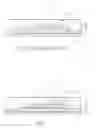
FIG. 1. is a cross-sectional view of a conventional flip chip-based SiP package having bond wires. Package 10 comprises a substrate 20 having first and second surfaces 30 and 40, respectively. A plurality of solder balls 110 are disposed on the first surface 30. A plurality of solder bumps 60 electrically connect the second surface 40 of the substrate 20 to an active surface of a large chip 50, such as for example a digital device. A small chip 80, such as an analog device, is stacked on a back surface of the large chip 50. Bond wires 90 electrically couple the small chip 80 to bond pads 95 on substrate 20.
To provide mechanical reinforcement to the large chip 50 and the substrate 20, an underfill material 70, such as resin, is typically dispensed in the gap between the large chip 50 and the substrate 20. This gap, if not underfilled, would easily cause the package 10 to suffer from fatigue cracking and electrical failure when it is being subjected to high-temperature conditions. One drawback to conventional underfill processes, however is that prior to the wire bonding process, the dispensed resin would easily flow wayward to nearby bond pads, contaminating them and making proper wire bonding of bond wires 90 to bond pads 95 difficult, if not impossible, resulting in yield loss. For this reason, chip package designers typically specify that a minimum distance A between an edge of the large chip 50 and the bond pad 95 of the substrate be more than 0.3 mm to avoid the underfill material overflowing the bond pads. However, due to this design rule constraint, designers are often not afforded design flexibility, which exacerbates the situation because they are precluded from manufacturing packages having reduced dimensions.
FIG. 1 shows a cross-sectional view of a SiP package where the underfill material 70 does not overflow on a bond pad 95. FIGS. 2A and 2B show examples of SiP packages depicting the overflow problem 120. FIG. 2A shows underfill material 70 overflowing a bond pad 95 in a flip chip-based SiP package; whereas FIG. 2B shows an adhesive material 75 overflowing a bond pad 95 in a wire bond SiP package.
For these reasons and other reasons that will become apparent upon reading the following detailed description, there is a need for an improved SiP package for minimizing bond wire contamination and yield loss and a method thereof that avoids the reliability concerns associate with conventional SiP packages.
SUMMARY
The present invention is directed to a system-in-package (SiP) package. In one embodiment, the SiP package comprises a substrate having a first surface and a second surface opposite the first surface, the substrate having a set of bond wire studs on bond pads formed on the second surface thereof; a first semiconductor chip having a first surface and a second surface opposite the first surface, wherein the first surface of the first semiconductor chip is mounted to the second surface of the substrate by means of solder bumps; an underfill material disposed between the first semiconductor chip and the substrate, encapsulating the solder bumps; a second semiconductor chip having a first surface and a second surface opposite the first surface, wherein the first surface of the second semiconductor chip is mounted to the second surface of the first semiconductor chip; and a set of bond wires electrically coupled from the second semiconductor chip to the set of bond wire studs on the substrate.
BRIEF DESCRIPTION OF THE DRAWINGS
The features, aspects, and advantages of the present invention will become more fully apparent from the following detailed description, appended claims, and accompanying drawings in which:
FIG. 1 is a cross-sectional view of a conventional SiP package.
FIGS. 2A-2B are cross-sectional views of conventional SiP packages used to depict a drawback of conventional wire bonding processes.
FIG. 3 is a cross-sectional view of a SiP package according to one embodiment of the present invention.
FIG. 4 is a detailed view of a bond wire stud employed in a SiP package according to one embodiment of the present invention.
FIG. 5 is a cross-sectional view of a SiP package according to another embodiment of the present invention.
DETAILED DESCRIPTION
In the following description, numerous specific details are set forth to provide a thorough understanding of the present invention. However, one having an ordinary skill in the art will recognize that the invention can be practiced without these specific details. In some instances, well-known structures and processes have not been described in detail to avoid unnecessarily obscuring the present invention.
Reference will now be made in detail to the present preferred embodiments of the present invention, examples of which are illustrated in the accompanying drawings.
FIG. 3 is a cross-sectional view of a SiP package according to one embodiment of the present invention. Package 10 comprises a substrate 20 having first and second surfaces 30 and 40, respectively. Substrate 20 can be a leadframe, PCB, or other well-known package substrates. A plurality of solder balls 110 may be disposed on the first surface 30 of the substrate 20 for coupling to another substrate (not shown). Substrate 20 has a set of bond wire studs 130 formed on the second surface thereof. Bond wire studs 130 may be formed on substrate 20 by conventional wire bonding and/or bump processes and may comprise of gold, copper, aluminum, alloys of the afore-mentioned metals, or other conductive metals as is known in the art. It is understood that bond wire studs 130 are formed on bond pads (sometimes also referred to as wire-bonding fingers) of substrate 20 before mounting a chip over the substrate. In this way, even if an underfill material or adhesive such as epoxy overflow onto the bond pad, so long as the top surface of the bond wire stud is exposed and there is enough wire bonding area thereon, a wire can be properly wire-bonded to a bond wire stud 130. The dimensions of the bond wire stud 130 will of course depend on design requirements; however, in one embodiment of the present invention, bond wire studs 130 have a height of between about 10 μm to about 30 μm high. In another embodiment, a space between an edge of the first semiconductor chip 55 and one of the set of bond wire studs 130 can be as small as 0.1 mm to about 0.2 mm. A detailed view B of a bond wire stud employed in a SiP package according to one embodiment of the present invention is shown in FIG. 4.
After formation of the set of bond wire studs 130 on the second surface 40 of substrate 20, the first semiconductor chip 55 is mounted in a flip-chip manner over the substrate 20 to reduce the package profile. The first semiconductor chip 55 has a first surface and a second surface opposite the first surface, wherein the first surface of the first semiconductor chip 55 is mounted to the second surface 40 of substrate 20 by means of a plurality of solder bumps 60. Solder bumps 60 can be solder, gold, copper, conductive organic materials, or other conductive materials as is known in the art. In other embodiments, wire-bonding (such as that shown in FIG. 5), tape-automatic bonding (TAB), or other known package technologies may be utilized to electrically connect the first semiconductor chip 55 to substrate 20.
Thereafter, an underfill material 70 is disposed between the first semiconductor chip 55 and the substrate 20 to encapsulate the solder bumps and enhance the structural rigidity and reliability of the package to buffer against thermal stresses induced by environmental factors such as thermal cycles. A predetermined amount of underfill material 70, such as resin, is directly dispensed in the gap between first semiconductor chip 55 and substrate 20. The dispensed resin will then fill into the gap through capillary action. It is understood that the resin may come in contact with the set of bond wire studs 130 but they do not flow over and/or overlap the top surfaces of the set of bond wire studs 130.
Following dispensation of the underfill material, a second semiconductor chip 85 is stacked on a back surface of the first semiconductor chip 55 by means of an adhesive, such as epoxy. By conventional wire bonding processes, a set of bond wires 90 electrically couple the second semiconductor chip 85 to the set of bond wire studs 130 on substrate 20. Thereafter, an encapsulant 100 such as a mixture of thermosetting epoxy, silica fillers, polyimide adhesive, or other materials as is known in the art encapsulates the first and second semiconductor chips, the set of bond wires, and the set of bond wire studs to prevent potential damage from moisture or other environmental contaminants.
In an alternative embodiment, as shown in FIG. 5, first semiconductor chip 55 is mounted onto substrate 20 by means of an adhesive 75, such as epoxy and another set of bond wires electrically connect the first semiconductor chip to the substrate by way of another set of bond wire studs.
The SiP package according to aspects of the present invention offers several advantages to the chip designer. First, the problem of yield loss caused by contamination and improper wire-bonding when the underfill or adhesive overflow to nearby bond pads is solved by the use of bond wire studs. Second, designers are given greater flexibility in chip designs because they are no longer constrained to design packages where the minimum distance between an edge of a large chip mounted on a substrate and a bond pad must be more than 0.3 mm. Accordingly, they are free to design packages having reduced dimensions.
In the preceding detailed description, the present invention is described with reference to specifically exemplary embodiments thereof. It will, however, be evident that various modifications, structures, processes, and changes may be made thereto without departing from the broader spirit and scope of the present invention, as set forth in the claims. The specification and drawings are, accordingly, to be regarded as illustrative and not restrictive. It is understood that the present invention is capable of using various other combinations and environments and is capable of changes or modifications within the scope of the inventive concept as expressed herein.
Claims
What is claimed is:1. A semiconductor package, comprising:
a substrate having a first surface and a second surface opposite the first surface, the substrate having a first and second set of bond wire studs on bond pads formed on the second surface thereof;
a first semiconductor chip having a first surface and a second surface opposite the first surface, wherein the first surface of the first semiconductor chip is mounted to the second surface of the substrate by means of an adhesive;
a second semiconductor chip having a first surface and a second surface opposite the first surface, wherein the first surface of the second semiconductor chip is mounted to the second surface of the first semiconductor chip;
a first set of bond wires electrically coupled from the first semiconductor chip to the first set of bond wire studs on the substrate; and
a second set of bond wires electrically coupled from the second semiconductor chip to the second set of bond wire studs on the substrate.
2. The semiconductor package of claim 1, wherein the adhesive does not flow over and overlap the top surfaces of the set of bond wire studs.
3. The semiconductor package of claim 1, wherein the first surface of the second semiconductor chip is mounted to the second surface of the first semiconductor chip by means of an adhesive.
4. The semiconductor package of claim 1, wherein a space between an edge of the first semiconductor chip and one of the sets of bond wire studs of the substrate is about 0.1 mm to about 0.2 mm.
5. The semiconductor package of claim 1, wherein a height of one of the sets of bond wire studs is between about 10 μm to about 30 μm high.
6. The semiconductor package of claim 1, further comprising an encapsulant that encapsulates the first and second semiconductor chips, the first and second sets of bond wires, and the first and second sets of bond wire studs.
7. A method for fabricating a system-in-package module, the method comprising:
providing a substrate having a first surface and a second surface opposite the first surface;
forming a set of bond wire studs on bond pads on the second surface of the substrate;
providing a first semiconductor chip having a first surface and a second surface opposite the first surface, wherein the first surface of the first semiconductor chip is mounted to the second surface of the substrate by means of solder bumps;
dispensing an underfill material between the first semiconductor chip and the substrate, encapsulating the solder bumps;
providing a second semiconductor chip having a first surface and a second surface opposite the first surface, wherein the first surface of the second semiconductor chip is mounted to the second surface of the first semiconductor chip; and
wire-bonding a set of bond wires from the second semiconductor chip to the set of bond wire studs on the substrate.
8. The method of claim 7, wherein the underfill material fills into the gap between the first semiconductor chip and the substrate through capillary action, and further wherein the underfill material does not flow over and overlap the top surfaces of the set of bond wire studs.
9. The method of claim 7, wherein a space between an edge of the first semiconductor chip and one of the set of bond wire studs of the substrate is about 0.1 mm to about 0.2 mm.
10. The method of claim 7, wherein a height of one of the set of bond wire studs is between about 10 μm to about 30 μm high.
11. A method for fabricating a system-in-package module, the method comprising:
providing a substrate having a first surface and a second surface opposite the first surface;
forming a first and second set of bond wire studs on bond pads on the second surface of the substrate;
providing a first semiconductor chip having a first surface and a second surface opposite the first surface, wherein the first surface of the first semiconductor chip is mounted to the second surface of the substrate by means of an adhesive;
providing a second semiconductor chip having a first surface and a second surface opposite the first surface, wherein the first surface of the second semiconductor chip is mounted to the second surface of the first semiconductor chip;
wire-bonding a first set of bond wires from the first semiconductor chip to the first set of bond wire studs on the substrate; and
wire-bonding a second set of bond wires from the second semiconductor chip to the second set of bond wire studs on the substrate.
12. The method of claim 11, wherein the adhesive does not flow over and overlap the top surfaces of the set of bond wire studs.
13. The method of claim 11, wherein a space between an edge of the first semiconductor chip and one of the sets of bond wire studs of the substrate is about 0.1 mm to about 0.2 mm.
14. The method of claim 11, wherein a height of one of the sets of bond wire studs is between about 10 μm to about 30 μm high.
Images & Drawings included:


Sources:
- United States Patent and Trademark Office - verify current appl. status at the USPTO↗
Similar patent applications:
Recent applications in this class:
- » 20250293212 2025-09-18
SEMICONDUCTOR PACKAGES - » 20250293211 2025-09-18
HEAT DISSIPATION FOR STACKED INTEGRATED CIRCUIT DEVICES - » 20250293210 2025-09-18
SYSTEMS AND METHODS FOR PACKAGING A SEMICONDUCTOR DEVICE - » 20250286021 2025-09-11
SEMICONDUCTOR PACKAGE - » 20250286020 2025-09-11
SEMICONDUCTOR BONDING STRUCTURE - » 20250286019 2025-09-11
SEMICONDUCTOR PACKAGE - » 20250286018 2025-09-11
METHOD OF FABRICATING SEMICONDUCTOR BONDING STRUCTURE - » 20250286017 2025-09-11
SEMICONDUCTOR DEVICE - » 20250279399 2025-09-04
SEMICONDUCTOR DEVICES AND MANUFACTURING METHODS OF THE SAME - » 20250279398 2025-09-04
VERTICAL INTERCONNECT STRUCTURES IN THREE-DIMENSIONAL INTEGRATED CIRCUITS
Recent applications for this Assignee:
- » 20240385384 2024-11-21
1D APODIZED GRATING DEVICES AND METHODS FOR SUPPRESSING OPTICAL NOISE - » 20240371674 2024-11-07
Method for PUF generation using variations in transistor threshold voltage and subthreshold leakage current - » 20240360950 2024-10-31
APPARATUS FOR STORING AND TRANSPORTING SEMICONDUCTOR ELEMENTS, AND METHOD OF MAKING THE SAME - » 20240321781 2024-09-26
ELECTROSTATIC DISCHARGE (ESD) ARRAY WITH CIRCUIT CONTROLLED SWITCHES - » 20240203997 2024-06-20
Integrated circuit device with improved layout - » 20240202374 2024-06-20
Method and apparatus for protecting a PUF generator - » 20240190701 2024-06-13
Methods for wafer bonding - » 20240154823 2024-05-09
Method and apparatus for noise injection for PUF generator characterization - » 20240153550 2024-05-09
Memory device including memory cells and edge cells - » 20240151908 2024-05-09
Fiber-to-chip grating coupler for photonic circuits