Circuit device
US20100188059A1
2010-07-29
12/667,031
2008-06-24
✅ Patent granted
US 8,363,419 B2
2013-01-29
WO; PCT/JP2008/001645; 20080624
WO; WO2009/001554; 20081231
Yuriy Semenenko
McDermott Will & Emery LLP
2029-06-04
Abstract:
An insulating resin layer (30) is formed on a metal substrate (20), and a wiring is formed on the insulating resin layer (30). A circuit composed of a circuit element (50) and a passive element (60) is formed on the wiring (40), and the metal substrate (20) is covered with an over coat (80) and a sealing resin member (90). The insulating resin layer (30) is provided with an opening (31) so that a part of the metal substrate (20) is exposed therefrom. The exposed part of the metal substrate (20) is connected to one terminal of a capacitor (62) through a conductive wire (42), and the other terminal of the capacitor (62) is connected to the ground potential.
Assignee:
- SANYO ELECTRIC CO., LTD. 4,445 🇯🇵 Osaka, Japan
Applicant:
Interested in similar patents?
Get notified when new applications in this technology area are published.
Classification:
H05K1/0231 » CPC main
Printed circuits; Details; Electrical arrangements not otherwise provided for; Reduction of cross-talk, noise or electromagnetic interference using auxiliary mounted passive components or auxiliary substances Capacitors or dielectric substances
H05K1/0231 » CPC main
Printed circuits; Details; Electrical arrangements not otherwise provided for; Reduction of cross-talk, noise or electromagnetic interference using auxiliary mounted passive components or auxiliary substances Capacitors or dielectric substances
H01L23/142 » CPC further
Details of semiconductor or other solid state devices; Mountings, e.g. non-detachable insulating substrates characterised by the material or its electrical properties Metallic substrates having insulating layers
H01L23/50 » CPC further
Details of semiconductor or other solid state devices; Arrangements for conducting electric current to or from the solid state body in operation, e.g. leads, terminal arrangements ; Selection of materials therefor for integrated circuit devices, e.g. power bus, number of leads
H01L23/642 » CPC further
Details of semiconductor or other solid state devices; Structural electrical arrangements for semiconductor devices not otherwise provided for, e.g. in combination with batteries; Impedance arrangements Capacitive arrangements
H01L25/165 » CPC further
Assemblies consisting of a plurality of individual semiconductor or other solid state devices ; Multistep manufacturing processes thereof the devices being of types provided for in two or more different main groups of - , e.g. forming hybrid circuits Containers
H01L24/45 » CPC further
Arrangements for connecting or disconnecting semiconductor or solid-state bodies; Methods or apparatus related thereto; Means for bonding being attached to, or being formed on, the surface to be connected, e.g. chip-to-package, die-attach, "first-level" interconnects; Manufacturing methods related thereto; Wire connectors; Manufacturing methods related thereto; Structure, shape, material or disposition of the wire connectors prior to the connecting process of an individual wire connector
H01L24/48 » CPC further
Arrangements for connecting or disconnecting semiconductor or solid-state bodies; Methods or apparatus related thereto; Means for bonding being attached to, or being formed on, the surface to be connected, e.g. chip-to-package, die-attach, "first-level" interconnects; Manufacturing methods related thereto; Wire connectors; Manufacturing methods related thereto; Structure, shape, material or disposition of the wire connectors after the connecting process of an individual wire connector
H01L2224/2612 » CPC further
Indexing scheme for arrangements for connecting or disconnecting semiconductor or solid-state bodies and methods related thereto as covered by; Means for bonding being attached to, or being formed on, the surface to be connected, e.g. chip-to-package, die-attach, "first-level" interconnects; Manufacturing methods related thereto; Layer connectors, e.g. plate connectors, solder or adhesive layers; Manufacturing methods related thereto Auxiliary members for layer connectors, e.g. spacers
H01L2224/73265 » CPC further
Indexing scheme for arrangements for connecting or disconnecting semiconductor or solid-state bodies and methods related thereto as covered by; Means for bonding being of different types provided for in two or more of groups; Location after the connecting process on different surfaces Layer and wire connectors
H01L2924/01012 » CPC further
Indexing scheme for arrangements or methods for connecting or disconnecting semiconductor or solid-state bodies as covered by; Chemical elements Magnesium [Mg]
H01L2924/01079 » CPC further
Indexing scheme for arrangements or methods for connecting or disconnecting semiconductor or solid-state bodies as covered by; Chemical elements Gold [Au]
H01L2924/19041 » CPC further
Indexing scheme for arrangements or methods for connecting or disconnecting semiconductor or solid-state bodies as covered by; Details of hybrid assemblies other than the semiconductor or other solid state devices to be connected; Structure; Component type being a capacitor
H01L2924/19105 » CPC further
Indexing scheme for arrangements or methods for connecting or disconnecting semiconductor or solid-state bodies as covered by; Details of hybrid assemblies other than the semiconductor or other solid state devices to be connected; Disposition of discrete passive components in a side-by-side arrangement on a common die mounting substrate
H01L2924/19107 » CPC further
Indexing scheme for arrangements or methods for connecting or disconnecting semiconductor or solid-state bodies as covered by; Details of hybrid assemblies other than the semiconductor or other solid state devices to be connected; Disposition of discrete passive components off-chip wires
H01L2924/3025 » CPC further
Indexing scheme for arrangements or methods for connecting or disconnecting semiconductor or solid-state bodies as covered by; Technical effects; Electrical effects Electromagnetic shielding
H05K1/056 » CPC further
Printed circuits; Details; Use of materials for the substrate; Insulated conductive substrates, e.g. insulated metal substrate the metal substrate being covered by an organic insulating layer
H05K1/056 » CPC further
Printed circuits; Details; Use of materials for the substrate; Insulated conductive substrates, e.g. insulated metal substrate the metal substrate being covered by an organic insulating layer
H05K3/284 » CPC further
Apparatus or processes for manufacturing printed circuits; Secondary treatment of printed circuits; Applying non-metallic protective coatings for encapsulating mounted components
H05K3/284 » CPC further
Apparatus or processes for manufacturing printed circuits; Secondary treatment of printed circuits; Applying non-metallic protective coatings for encapsulating mounted components
H05K3/4046 » CPC further
Apparatus or processes for manufacturing printed circuits; Forming printed elements for providing electric connections to or between printed circuits; Through-connections; Vertical interconnect access [VIA] connections using auxiliary conductive elements, e.g. metallic spheres, eyelets, pieces of wire
H05K2201/09554 » CPC further
Indexing scheme relating to printed circuits covered by; Shape and layout; Shape and layout details of conductors; Conductive through-holes or vias Via connected to metal substrate
H05K2201/09554 » CPC further
Indexing scheme relating to printed circuits covered by; Shape and layout; Shape and layout details of conductors; Conductive through-holes or vias Via connected to metal substrate
H05K2201/10287 » CPC further
Indexing scheme relating to printed circuits covered by; Details of components or other objects attached to or integrated in a printed circuit board; Other objects, e.g. metallic pieces Metal wires as connectors or conductors
H05K2201/10287 » CPC further
Indexing scheme relating to printed circuits covered by; Details of components or other objects attached to or integrated in a printed circuit board; Other objects, e.g. metallic pieces Metal wires as connectors or conductors
H01L2924/00014 » CPC further
Indexing scheme for arrangements or methods for connecting or disconnecting semiconductor or solid-state bodies as covered by; Technical content checked by a classifier the subject-matter covered by the group, the symbol of which is combined with the symbol of this group, being disclosed without further technical details
H01L2924/00015 » CPC further
Indexing scheme for arrangements or methods for connecting or disconnecting semiconductor or solid-state bodies as covered by; Technical content checked by a classifier the subject-matter covered by the group, the symbol of which is combined with the symbol of this group, being disclosed as prior art
H01L2924/181 » CPC further
Indexing scheme for arrangements or methods for connecting or disconnecting semiconductor or solid-state bodies as covered by; Details of package parts other than the semiconductor or other solid state devices to be connected Encapsulation
H01L2924/00 » CPC further
Indexing scheme for arrangements or methods for connecting or disconnecting semiconductor or solid-state bodies as covered by
G05F1/10 IPC
Automatic systems in which deviations of an electric quantity from one or more predetermined values are detected at the output of the system and fed back to a device within the system to restore the detected quantity to its predetermined value or values, i.e. retroactive systems Regulating voltage or current
H02M3/06 IPC
Conversion of dc power input into dc power output without intermediate conversion into ac by static converters using resistors or capacitors, e.g. potential divider
H05K1/18 IPC
Printed circuits Printed circuits structurally associated with non-printed electric components
H05K1/18 IPC
Printed circuits Printed circuits structurally associated with non-printed electric components
Description
TECHNICAL FIELD
The present invention relates to a circuit device. More specifically, the invention relates to a circuit device having circuit elements disposed on an insulating resin layer on a metal substrate.
BACKGROUND TECHNOLOGY
In recent years, the power module has been in growing demand for smaller size and better heat release in order to achieve improved space efficiency. Also, there has been demand for lower energy cost and reduced environmental load of the power module. Developed to meet these demands are intelligent power modules (IPMs), which are circuit devices having both a control unit and a power device mounted on a single metal substrate.
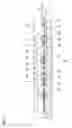
FIG. 11 is a cross-sectional view schematically illustrating a structure of a conventional circuit device. An insulating resin layer 510 is formed on a metal substrate 500 made of aluminum or the like. Wirings 520 made of copper, for instance, are formed on the insulating resin layer 510. Further, circuit elements 530, such as transistors and ICs, and passive elements 540, such as resistors and capacitors, are mounted on the wirings 520 through the medium of solder 551, thereby realizing a predetermined circuit. When the circuit elements 530 are to be mounted face-up, the electrodes of the circuit elements 530 are connected to the wirings 520 by wire bonding using gold wire 532. An external lead 550 is connected to an external electrode terminal 552 through the medium of solder 551, and a part of the external lead 550 is exposed outside from a sealing resin member 580 to be described later.
Note that the insulating resin layer 510 is provided with an opening which allows a part of the metal substrate 500 to be exposed. The exposed part of the metal substrate 500 is connected to a wiring 520a which is connected to ground potential. As a result, the metal substrate 500 functions as a shield even when the circuit elements 530 are in operation, so that malfunction of the circuit and occurrence of noise are being suppressed.
An overcoat 560 is formed to cover solder joints, gold wires 532, circuit elements 530, and passive elements 540.
The sealing resin member 580 includes a support 582 and a sealing resin layer 584. The support 582 and the sealing resin layer 584 are both made of a thermoplastic resin. The sealing resin 580 is formed by injection molding in which the metal substrate 500 placed on the support 582 is coated with the sealing resin layer 584. This produces a circuit device of a full-molded structure.
[Patent Document 1] Japanese Patent Application Publication No. 2005-277174.
DISCLOSURE OF THE INVENTION
Problems to be Solved by the Invention
In a conventional circuit device as shown in FIG. 11, even when a capacitance is produced between the wiring 520 and the metal substrate 500, there results no variation in the potential of the metal substrate 500 because the metal substrate 500 is connected to ground potential. This has the effects of preventing an amplifier circuit or the like from malfunctioning due to noise. Nevertheless, when the metal substrate 500 is connected to ground potential, it is necessary to coat the metal substrate 500 with an insulator in order to prevent short-circuiting therethrough. And the coating of the metal substrate 500 with the insulator results in a drop in the heat transference of the metal substrate 500, which in turn lowers the heat release performance of the circuit device as a whole.
The present invention has been made in view of these problems to be solved, and a purpose thereof is to provide a technology for structuring a circuit device, having circuit elements disposed on an insulating resin layer on a metal substrate, which can prevent the “sneaking in” of noise from a circuit element into another circuit element through the metal substrate without causing a loss of heat release performance of the metal substrate.
Means for Solving the Problems
One embodiment of the present invention relates to a circuit device. This circuit device comprises: a metal substrate; an insulating resin layer disposed on the metal substrate; a wiring disposed on the insulating resin layer; a circuit element disposed on the wiring; and a capacitor, one terminal thereof being connected to the metal substrate and the other terminal thereof being connected to a fixed potential.
Another embodiment of the present invention relates also to a circuit device. This circuit device comprises: a metal substrate; an insulating resin layer disposed on the metal substrate; a wiring disposed on the insulating resin layer; a circuit element disposed on the wiring; and a capacitor, one terminal thereof being connected to the metal substrate and the other terminal thereof being connected to a variation potential which varies in such a manner as to cancel the potential of the metal substrate. In this embodiment, the variation potential may be in reverse phase with the potential of the circuit element.
Still another embodiment of the present invention relates also to a circuit device. This circuit device comprises: a metal substrate; an insulating resin layer disposed on the metal substrate; a wiring disposed on the insulating resin layer; a circuit element disposed on the wiring; and a means which applies a voltage, used to offset the potential of the metal substrate, to the metal substrate when the potential of the metal substrate varies, so as to maintain the potential of the metal substrate at ground level.
Still another embodiment of the present invention relates also to a circuit device. This circuit device comprises: a metal substrate; an insulating resin layer disposed on the metal substrate; a wiring disposed on the insulating resin layer; a circuit element disposed on the wiring; and a resistor, one terminal thereof being connected to the metal substrate and the other terminal thereof being connected to a fixed potential. In this embodiment, the resistor may be cut off when a current which is greater than a reference current flows.
Optional combinations of the aforementioned constituting elements may also be within the scope of the invention protected by the present patent application.
EFFECT OF THE INVENTION
According to the present invention, a circuit device, having circuit elements disposed on an insulating layer on a metal substrate, can prevent the “sneaking in” of noise from a circuit element into another circuit element through the metal substrate without causing a loss of heat radiating performance of the metal substrate.
BRIEF DESCRIPTION OF THE DRAWINGS
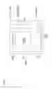
FIG. 1 is a schematic illustration of an inverter module where a circuit device according to a first embodiment of the present invention is used.
FIG. 2 is a schematic diagram showing a structure of an inverter module.
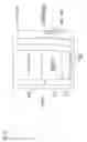
FIG. 3 is a cross-sectional view schematically showing a structure of a circuit device according to a first embodiment of the present invention.
FIG. 4 is a schematic illustration showing capacitive coupling through a metal substrate in a circuit device according to a first embodiment.
FIG. 5 is a graph showing the measurements of the voltage of an input signal, the voltage of an output signal, and the potential of a metal substrate when a capacitor is not connected to the metal substrate.
FIG. 6 is a graph showing the measurements of the voltage of an input signal, the voltage of an output signal, and the potential of a metal substrate when a capacitor is connected to the metal substrate.
FIG. 7 is a graph showing the measurements of the potential in reverse phase, the voltage of an output signal, and the potential of a metal substrate when one end of a capacitor is connected to a potential in reverse phase with the output signal of a power element.
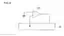
FIG. 8 shows a configuration of a circuit that contains a differential amplifier used in a circuit device according to a fourth embodiment of the present invention.
FIG. 9 shows a configuration of a circuit that contains a differential amplifier when the potential variation of a metal substrate due to noise is sufficiently behind the operating frequency of circuit elements.
FIG. 10 is a cross-sectional view schematically showing a structure of a circuit device according to a fifth embodiment of the present invention.
FIG. 11 is a cross-sectional view schematically showing a structure of a conventional circuit device.
DESCRIPTION OF THE REFERENCE NUMERALS
-
- 10 Circuit device
- 20 Metal substrate
- 30 Insulating resin layer
- 40 Wiring
- 50 Circuit element
- 52 Gold wire
- 60 Passive element
- 70 External lead
- 71 Soldering
- 72 External electrode terminal
- 80 Overcoat
- 90 Sealing resin member
BEST MODE FOR CARRYING OUT THE INVENTION
First Embodiment
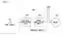
FIG. 1 is a schematic illustration of an inverter module where a circuit device according to a first embodiment of the present invention is used. FIG. 2 is a schematic diagram showing a structure of the inverter module. PWM (Pulse Width Modulation) signals are inputted to an inverter module 400. The PWM signal inputted to the inverter module 400 is normally at a logic level (5V). The inverter module 400 includes a voltage amplifier unit 410 and a power amplifier unit 420, and the PWM signal of 5 V is voltage-amplified and power-amplified to the PWM signal of 500 V so as to drive a motor 430. The three-phase motor 430 requires three phases which are U-phase, V-phase and W-phase. The voltage amplifier unit 410 has booster circuits 412, 414 and 416 corresponding to the U-phase, the V-phase and the W-phase, respectively. The power amplifier unit 420 has power elements 421 and 424 corresponding to the U-phase, power elements 422 and 425 corresponding to the V-phase, and power elements 423 and 426 corresponding to the W-phase.
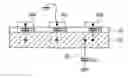
FIG. 3 is a cross-sectional view schematically showing a structure of a circuit device 10 according to the first embodiment of the present invention. As shown in FIG. 3, an insulating resin layer 30 is formed on a metal substrate 20 in the circuit device 10 according to the first embodiment.
An example of the metal substrate 20 is a cladding material where a lower metal layer made of a metal, such as aluminum and copper, an alloy and copper, an intermediate metal layer, formed on the lower metal layer, which is made of a Fe—Ni-based alloy (so-called inver alloy), and an upper metal layer, formed on the intermediate metal layer, which is made of copper are stacked together.
The material used to form the insulating resin layer 30 is, for instance, a melamine derivative, such as BT resin, or a thermosetting resin, such as liquid-crystal polymer, epoxy resin, PPE resin, polyimide resin, fluorine resin, phenol resin or polyamide bismaleimide. From the viewpoint of improving the heat radiation of the circuit device 10, it is desirable that the insulating resin layer 30 has a high thermal conductivity. In this respect, it is preferable that the insulating resin layer 30 contains, as a high thermal conductive filler, silver, bismuth, copper, aluminum, magnesium, tin, zinc, or an alloy thereof.
Wirings 40 made of copper, for instance, is formed on the insulating resin layer 30. Further, circuit elements 50 such as transistors and ICs, and passive elements 60, such as resistors and capacitors, are mounted on the wirings 40 through the medium of solder 71, thereby realizing a predetermined circuit. When the circuit elements 50 are to be mounted face-up, the electrodes of the circuit elements 50 are connected to the wirings 40 by wire bonding using gold wire 52. An external lead 70 is connected to an external electrode terminal 72 through the medium of solder 71, and a part of the external lead 70 is exposed outside from a sealing resin member 90 to be described later.
In the present embodiment, a capacitor 62 is mounted on wirings 40a and 40b through the medium of solder 71. One terminal of the capacitor 62 is connected to the wiring 40a via the solder 71. At the same time, the other terminal of the capacitor is connected to the wiring 40b via the solder 71.
An opening 31 is formed in the insulating resin layer 30 so that a part of the metal substrate is exposed thereon. The exposed part of the metal substrate 20 is connected to the wiring 40a via a conductive wire 42. That is, one terminal of the capacitor 62 is connected to the metal substrate 20. At the same time, the wiring 40b is connected is connected to ground potential. That is, the other terminal of the capacitor 62 is connected to ground potential. Though in the present embodiment the other terminal of the capacitor 62 is connected to ground potential, the other terminal of the capacitor 62 may be connected to a fixed potential. Note that the fixed potential may be, for example, ground potential or a potential such as the power supply voltage of an amplifier and therefore may be either a positive or negative potential.
An overcoat 80 is so formed as to cover solder joints, the gold wire 52, the circuit elements 50, and the passive elements 60. The overcoat 80 is formed, using a thermosetting resin (e.g., epoxy resin), by a potting process. Provision of the overcoat 80 prevents fine wires (about 30 to 80 μm in thickness) from falling and being disconnected due to the resin injection pressure applied when the sealing resin member 90 is formed. Also, the overcoat 80 prevents the solder 71 from melting and causing defects due to an injection temperature of about 300° C. when the sealing resin member 90 is formed.
The sealing resin member 90 is made of a thermoplastic resin. The sealing resin member 90 is formed by injection molding in which the metal substrate 20 is coated with the thermoplastic resin. Note that the lower surface of the metal substrate 20 is not coated with the sealing resin member 90 and is therefore exposed.
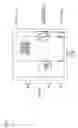
FIG. 4 is a schematic illustration showing capacitive coupling through a metal substrate 20 in a circuit device according to the first embodiment. In this schematic illustration, a power element 100, a circuit element 102 (fixed node) with a fixed potential, and a circuit element 104 susceptible to the effects of potential variation are presented as examples of circuit elements mounted on the insulating resin layer 30.
The power element 100 corresponds to an active channel outputting a PWM signal among the six channels (power elements) in the inverter module shown in FIG. 2, for instance. The circuit element 102 corresponds to an inactive channel with a fixed potential among the six channels or a power source. The circuit element 104 corresponds to a circuit element constituting a booster circuit preceding the active channel.
It should be noted that the circuit element 104 is not limited to a digital circuit element used as a booster circuit in the inverter module mentioned above, and the circuit element 104 may also be an analog circuit element used as an amplifier for amplifying inputted analog signals. When the circuit element 104 is an amplifier for amplifying inputted analog signals, however, there may occur a variation in the potential of the metal substrate 20 due to the effects of the outputted analog signals. Then the SN ratio (signal-to-noise ratio) may get worse on account of noise entering in the different amplification stages of the amplifier.
Assume that C1 is the capacitance of a hypothetical capacitor formed between the power element 100 and the metal substrate 20 through the medium of the insulating resin layer 30. Assume that C2 is the capacitance of a hypothetical capacitor formed between the circuit element 102 connected to ground potential through the insulating resin layer 30 and the metal substrate 20. Also, assume that C3 is the capacitance of a hypothetical capacitor formed between a circuit element 104 node and the metal substrate 20 through the medium of the insulating resin layer 30. In addition, assume that Cad is the capacitance of a capacitor 62 connected between the metal substrate 20 and ground potential.
The potential of the metal substrate 20 changes under the effects of voltage of the power element 100. The potential variation of the metal substrate 20 becomes noise to the circuit element 104. On account of this noise, the circuit element 104 can malfunction. According to the present embodiment, however, the metal substrate 20 is connected to the capacitor 62 which is connected to ground potential at the other terminal thereof, so that the potential variation of the metal substrate 20 is reduced with the result of reduced likelihood of the circuit element 104 malfunctioning.
Now the potential control effect of the capacitor 62 on the metal substrate 20 will be explained. Firstly, let ΔVn denote the voltage variation of the power element 100, which is the noise source, and ΔVb denote the potential variation of the metal substrate 20. Then the following equation holds:
(ΔVn−ΔVb)−C1=ΔVb×(C2+Cad) (1)
From this equation, the following equation can be derived:
ΔVb=(C1/(C1+C2+Cad))×ΔVn (2)
The noise the circuit element 104 is exposed to is in proportion to ΔVb. From Equation (2), therefore, it is evident that ΔVb can be reduced by the choice of larger Cad, and by extension it is possible to prevent the malfunction of the circuit element 104.
(Experimental Example of Three-Phase Inverter Module)
The potential suppression effect of the metal substrate 20 when the above-described capacitor 62 is connected thereto has been checked using a three-phase inverter module. Specifically, the capacitance of the capacitor 62 used was 9400 pF (Two capacitors of 4700 pF each were used). For comparison, a checking has been done of the potential variation of the metal substrate 20 when the metal substrate 20 is not connected to the capacitor 62, that is, when the metal substrate 20 is in a floating state. Note that the amplitude of the PWM signal inputted was 5 V.
FIG. 5 is a graph showing the measurements of the voltage of an input signal, the voltage of an output signal, and the potential of the metal substrate when the capacitor 62 is not connected to the metal substrate 20. FIG. 6 is a graph showing the measurements of the voltage of an input signal, the voltage of an output signal, and the potential of the metal substrate when the capacitor 62 is connected to the metal substrate 20. As shown in FIG. 5, when the capacitor 62 was not connected to the metal substrate 20, the potential variation of the metal substrate was about 17 V with the amplitude of the output signal set to 120 V, and malfunctions occurred with the amplitude of the output signal amplified to 125 V or above. In contrast to this, as shown in FIG. 6, when the capacitor 62 was connected to the metal substrate 20, it has been confirmed that with the amplitude of the output signal amplified to 450 V, the potential variation of the metal substrate was suppressed to about 6 V and no malfunctions occurred.
In a circuit device according to the present embodiment heretofore described, the potential variation of the metal substrate is reduced by a capacitor connected between the metal substrate and ground potential, so that it is possible to reduce the “sneaking in” of noise from a high-voltage circuit element, such as a power element, into another circuit element which is susceptible to the effect of potential variation.
Also, since the metal substrate is not connected directly to ground potential, a large current will not flow even if an external object comes in contact with the metal substrate. Accordingly, the circuit device in the present embodiment can have part of the metal substrate exposed. With a part of the metal substrate exposed, it is possible to reduce thermal resistance and improve the heat release performance of the circuit device.
Second Embodiment
The structure of a circuit device according to a second embodiment of the present invention is substantially the same as that of the first embodiment. The circuit device according to the present embodiment differs, however, in that one end of the capacitor 62 connected to the metal substrate 20 shown in FIG. 3 is not connected to ground potential but to a potential in reverse phase with the output signal of a power element. The potential in reverse phase with the output signal of the power element can be taken, for instance, from a midway stage of an amplifier amplifying the input signal. In this arrangement, the potential variation of the metal substrate 20 due to the output signal of the power element can be offset by the capacitor 62, so that the potential variation of the metal substrate 20 can be reduced more effectively. Thus, for a capacitance of the capacitor 62 smaller than that of the first embodiment, a sufficient noise reduction effect can be achieved.
(Experimental Example of Three-Phase Inverter Module)
The potential suppression effect of the metal substrate 20 when one end of the capacitor 62 shown in FIG. 3 is connected to a potential (amplitude: 5 V) in reverse phase with the output signal of a power element has been checked using a three-phase inverter module. FIG. 7 is a graph showing the measurements of the potential in reverse phase, the voltage of an output signal, and the potential of the metal substrate when one end of the capacitor 62 is connected to a potential in reverse phase with the output signal of the power element. As shown in FIG. 7, when one end of the capacitor 62 is connected to a potential in reverse phase with the output signal of the power element, it has been confirmed that the potential variation of the metal substrate with the amplitude of the output signal amplified to 450 V was suppressed to about 1 to 2 V, which represents even smaller potential variation of the metal substrate than that in the first embodiment.
Experiments were conducted on the structures of the first embodiment and the second embodiment by halving the capacitance of the capacitor 62 shown in FIG. 3 (namely with the capacitor 62 of 4700 pF). In the first embodiment, malfunctions occurred when the output voltage of the power element was 397 V or above. In contrast to this, in the second embodiment, it has been confirmed that the operation was normal even when the output voltage of the power element was raised to 450 V. In other words, with the circuit device of the second embodiment, it has been confirmed that even when the capacitance of the capacitor 62 is made smaller than that of the first embodiment, a sufficient noise reduction effect can be achieved.
Third Embodiment
The structure of a circuit device according to a third embodiment of the present invention is substantially the same as that of the first embodiment. The circuit device according to the present embodiment differs, however, in that one end of the capacitor 62 connected to the metal substrate 20 shown in FIG. 3 is not connected to ground potential but to a control potential that is determined in accordance with the potential variation of the metal substrate 20. Specifically, a potential detecting means (not shown) for detecting the potential variation of the metal substrate 20 is provided, and when a potential variation of the metal substrate 20 is detected by the potential detecting means, a potential that can cancel the potential of the metal substrate 20 is set as the control potential. This further reduces the potential variation of the metal substrate 20, so that the noise reduction effect can be further enhanced.
Fourth Embodiment
The structure of a circuit device according to a fourth embodiment of the present invention is substantially the same as that of the first embodiment. The circuit device according to the present embodiment differs, however, in that a differential amplifier is provided in the place of the capacitor 62 connected to the metal substrate 20 shown in FIG. 3. Specifically, as shown in FIG. 8, one input terminal (−) of a differential amplifier 110 is connected to the metal substrate 20, the other input terminal (+) of the differential amplifier 110 is connected to ground potential, and the output terminal of the differential amplifier 110 is connected to the metal substrate 20. When there is a change in potential of the metal substrate 20 due to noise from a power element or the like, the differential amplifier 110 works in such a manner as to cancel the potential variation, thereby maintaining the potential of the metal substrate 20 at ground level. With the potential of the metal substrate 20 maintained at ground level, the noise reduction effect can be further enhanced.
Note that when the potential variation of the metal substrate due to noise is sufficiently behind the operating frequency of circuit elements, the effects of noise can be ignored. Therefore, it is only the noise of a certain frequency or above affecting the operation of circuit elements that must be dealt with, and hence capacitors 120 capable of cutting the DC components of the noise may be inserted in the respective nodes to set the metal substrate in a floating state.
Fifth Embodiment
The structure of a circuit device according to a fifth embodiment of the present invention is substantially the same as that of the first embodiment. The circuit device according to the present embodiment differs, however, in that, as shown in FIG. 10, a resistor 66 (50Ω, for instance) is provided in the place of the capacitor 62 connected to the metal substrate 20 shown in FIG. 3. And one end of the resistor 66 is connected to the metal substrate 20, whereas the other end of the resistor 66 is connected to ground potential. According to this arrangement, the noise of the metal substrate 20 is discharged by the resistor, so that the potential of the metal substrate 20 is maintained at ground level. In case where a short-circuiting should occur due to the exposure of the metal substrate 20, the current will be limited by the resistor 66, and therefore there will be reduced likelihood of damage to an external circuit or the like coming into contact with the metal substrate 20.
It is preferable that the resistor 66 functions as a fuse blowing when a large current above a predetermined current flows. In such an arrangement, if an overcurrent flows due to a short-circuiting or the like, the resistor 66 will be severed to prevent electric shock.
The present invention has been described by referring to each of the above-described embodiments. However, the present invention is not limited to the above-described embodiments only, and various modifications, such as changes in design, are possible. The embodiments added with such modifications are also within the scope of the present invention.
For the purpose of noise reduction, for instance, a capacitor is used in the first to third embodiments, and a resistor in the fifth embodiment. However, a capacitor and a resistor may be used in combination.
INDUSTRIAL APPLICABILITY
The present invention may find its application in the fabrication of circuit devices having circuit elements disposed on an insulating resin layer on a metal substrate.
Claims
1-6. (canceled)
7. A circuit device, comprising:
a metal substrate;
an insulating resin layer disposed on said metal substrate;
a wiring disposed on said insulating resin layer;
a circuit element disposed on said wiring; and
a capacitor, one terminal thereof being connected to said metal substrate and the other terminal thereof being connected to a fixed potential,
wherein said metal substrate is set to a potential other than the fixed potential, and
wherein the potential other than the fixed varies.
8. A circuit device, comprising:
a metal substrate;
an insulating resin layer disposed on said metal substrate;
a wiring disposed on said insulating resin layer;
a circuit element disposed on said wiring; and
a capacitor, one terminal thereof being connected to said metal substrate and the other terminal thereof being connected to a variation potential which varies in such a manner as to cancel the potential of the metal substrate.
9. A circuit device according to claim 8, wherein the variation potential is in reverse phase with the potential of the circuit element.
10. A circuit device, comprising:
a metal substrate;
an insulating resin layer disposed on said metal substrate;
a wiring disposed on said insulating resin layer;
a circuit element disposed on said wiring; and
a means which applies a voltage, used to cancel the potential of the metal substrate, to the metal substrate when the potential of the metal substrate varies, so as to maintain the potential of the metal substrate at a fixed level.
11. A circuit device, comprising:
a metal substrate;
an insulating resin layer disposed on said metal substrate;
a wiring disposed on said insulating resin layer;
a circuit element disposed on said wiring; and
a resistor, one terminal thereof being connected to said metal substrate and the other terminal thereof being connected to a fixed potential.
12. A circuit device according to claim 11, wherein when a current which is greater than a reference current flows, the resistor is cut off.
Images & Drawings included:


Sources:
- United States Patent and Trademark Office - verify current appl. status at the USPTO↗
Similar patent applications:
- » 10790293
Circuit devices, circuit devices which include light emitting diodes, assemblies which include such circuit devices, flashlights which include such assemblies, and methods for directly replacing flashlight bulbs - » 20070285149
Switch circuit device, and wireless circuit device and sampling circuit device employing the same - » 20130322888
OPTICAL TRANSMISSION CIRCUIT DEVICE, OPTICAL RECEPTION CIRCUIT DEVICE, OPTICAL TRANSMISSION/RECEPTION CIRCUIT DEVICE AND OPTICAL TRANSMISSION METHOD - » 20080028349
Method for identifying semiconductor integrated circuit device, method for manufacturing semiconductor integrated circuit device, semiconductor integrated circuit device and semiconductor chip - » 10660098
Molecular device, molecule array, rectifier device, rectifying method, sensor device, switching device, circuit device, logical circuit device, operational device and information processing device - » 20050175984
Molecular device, molecule array, rectifier device, rectifying method, sensor device, switching device, circuit device, logical circuit device, operational device and information processing device - » 10433161
Method for identifying semiconductor integrated circuit device, method for manufacturing semiconductor integrated circuit device, semiconductor integrated circuit device and semiconductor chip - » 20050263605
Method for identifying semiconductor integrated circuit device, method for manufacturing semiconductor integrated circuit device, semiconductor integrated circuit device and semiconductor chip - » 20090249264
Analyzing device for circuit device, circuit device analyzing method, analyzing program, and electronic medium - » 20240372444
METHOD FOR PRODUCING AN ELECTRICAL CIRCUIT DEVICE FOR OPERATING AN EXTERNALLY EXCITED ELECTRIC MACHINE, ELECTRICAL CIRCUIT DEVICE FOR OPERATING AN EXTERNALLY EXCITED ELECTRIC MACHINE, ELECTRIC DRIVE DEVICE COMPRISING AN ELECTRICAL CIRCUIT DEVICE, AND MOTOR VEHICLE COMPRISING AN ELECTRIC DRIVE DEVICE
Recent applications in this class:
- » 20250254788 2025-08-07
IN-LINE CAPACITOR MODULE - » 20250142713 2025-05-01
Component Carrier With Embedded Electronic Switch Components and a Capacitor Device - » 20250081329 2025-03-06
WIRING BOARD AND LAMINATED WIRING BOARD - » 20250056712 2025-02-13
MANUFACTURING METHOD OF CIRCUIT BOARD - » 20240422895 2024-12-19
STRUCTURALLY ENHANCED FILTERING OF CIRCUIT BOARD PLANES - » 20240365464 2024-10-31
CIRCUIT BOARD, ELECTRONIC DEVICE, AND METHOD OF MANUFACTURING CIRCUIT BOARD - » 20240334591 2024-10-03
MODULE AND SEMICONDUCTOR COMPOSITE APPARATUS - » 20240314924 2024-09-19
CONTROL CIRCUIT AND POWER SUPPLY DEVICE - » 20240306288 2024-09-12
ELECTRONIC DEVICE - » 20240107661 2024-03-28
Signal processing board and image forming apparatus
Recent applications for this Assignee:
- » 20250231288 2025-07-17
POWER SUPPLY DEVICE, ELECTRIC VEHICLE USING SAME, AND POWER STORAGE DEVICE - » 20250192345 2025-06-12
SECONDARY BATTERY - » 20250096278 2025-03-20
RECTANGULAR SECONDARY BATTERY AND METHOD OF MANUFACTURING THE SAME - » 20250055043 2025-02-13
PRISMATIC SECONDARY BATTERY AND ASSEMBLED BATTERY USING THE SAME - » 20250038213 2025-01-30
SLURRY FOR NON-AQUEOUS ELECTROLYTE SECONDARY CELL, METHOD FOR MANUFACTURING SLURRY FOR NON-AQUEOUS ELECTROLYTE SECONDARY CELL, ELECTRODE FOR NON-AQUEOUS ELECTROLYTE SECONDARY CELL, AND NON-AQUEOUS ELECTROLYTE SECONDARY CELL - » 20240297386 2024-09-05
BATTERY PACK - » 20240283051 2024-08-22
BATTERY MODULE - » 20240213513 2024-06-27
ELECTRICITY STORAGE DEVICE COMPRISING A COVERING MEMBER FOR A LIQUID INJECTION HOLE - » 20240204339 2024-06-20
GAS DISCHARGE VALVE OF BATTERY AND BATTERY - » 20240204259 2024-06-20
NON-AQUEOUS ELECTROLYTE SECONDARY BATTERY