Occam process for components having variations in part dimensions
US20110315302A1
2011-12-29
13/228,826
2011-09-09
✅ Patent granted
US 9,894,771 B2
2018-02-13
-
-
Michael N Orlando | Marta S Dulko
Edward P Heller, III
2033-02-11
Abstract:
An Occam process (solderless manufacturing) that employs a component support fixture that provides permanent or temporary support for components during subsequent processing in a solderless process for electrically connecting the components to circuits. The component support fixture provides oversized compartments for housing the components which may have varying sizes. The compartments are provided with vent holes or apertures for venting air or excess glue as the component support is pressed against the components during manufacture.
Assignee:
- OCCAM PORTFOLIO LLC 20 🇺🇸 Cupertino, CA, United States
Applicant:
Interested in similar patents?
Get notified when new applications in this technology area are published.
Classification:
H01L2924/00014 » CPC further
Indexing scheme for arrangements or methods for connecting or disconnecting semiconductor or solid-state bodies as covered by; Technical content checked by a classifier the subject-matter covered by the group, the symbol of which is combined with the symbol of this group, being disclosed without further technical details
B32B2307/202 » CPC further
Properties of the layers or laminate having particular electrical or magnetic properties, e.g. piezoelectric Conductive
H01L2924/00013 » CPC further
Indexing scheme for arrangements or methods for connecting or disconnecting semiconductor or solid-state bodies as covered by; Technical content checked by a classifier Fully indexed content
H01L2924/01013 » CPC further
Indexing scheme for arrangements or methods for connecting or disconnecting semiconductor or solid-state bodies as covered by; Chemical elements Aluminum [Al]
H01L2924/14 » CPC further
Indexing scheme for arrangements or methods for connecting or disconnecting semiconductor or solid-state bodies as covered by; Details of semiconductor or other solid state devices to be connected; Device type Integrated circuits
B32B37/02 IPC
Methods or apparatus for laminating, e.g. by curing or by ultrasonic bonding characterised by a sequence of laminating steps, e.g. by adding new layers at consecutive laminating stations
H01L2224/29099 » CPC further
Indexing scheme for arrangements for connecting or disconnecting semiconductor or solid-state bodies and methods related thereto as covered by; Means for bonding being attached to, or being formed on, the surface to be connected, e.g. chip-to-package, die-attach, "first-level" interconnects; Manufacturing methods related thereto; Layer connectors, e.g. plate connectors, solder or adhesive layers; Manufacturing methods related thereto; Structure, shape, material or disposition of the layer connectors prior to the connecting process of an individual layer connector; Core members of the layer connector Material
H01L2924/00 » CPC further
Indexing scheme for arrangements or methods for connecting or disconnecting semiconductor or solid-state bodies as covered by
H05K1/189 » CPC main
Printed circuits; Printed circuits structurally associated with non-printed electric components characterised by the use of a flexible or folded printed circuit
H05K1/189 » CPC main
Printed circuits; Printed circuits structurally associated with non-printed electric components characterised by the use of a flexible or folded printed circuit
B32B37/153 » CPC further
Methods or apparatus for laminating, e.g. by curing or by ultrasonic bonding characterised by the properties of the layers with at least one layer being manufactured and immediately laminated before reaching its stable state, e.g. in which a layer is extruded and laminated while in semi-molten state at least one layer is extruded and immediately laminated while in semi-molten state
H01L24/29 » CPC further
Arrangements for connecting or disconnecting semiconductor or solid-state bodies; Methods or apparatus related thereto; Means for bonding being attached to, or being formed on, the surface to be connected, e.g. chip-to-package, die-attach, "first-level" interconnects; Manufacturing methods related thereto; Layer connectors, e.g. plate connectors, solder or adhesive layers; Manufacturing methods related thereto; Structure, shape, material or disposition of the layer connectors prior to the connecting process of an individual layer connector
H01L24/32 » CPC further
Arrangements for connecting or disconnecting semiconductor or solid-state bodies; Methods or apparatus related thereto; Means for bonding being attached to, or being formed on, the surface to be connected, e.g. chip-to-package, die-attach, "first-level" interconnects; Manufacturing methods related thereto; Layer connectors, e.g. plate connectors, solder or adhesive layers; Manufacturing methods related thereto; Structure, shape, material or disposition of the layer connectors after the connecting process of an individual layer connector
H01L24/83 » CPC further
Arrangements for connecting or disconnecting semiconductor or solid-state bodies; Methods or apparatus related thereto; Methods for connecting semiconductor or other solid state bodies using means for bonding being attached to, or being formed on, the surface to be connected using a layer connector
H01L24/93 » CPC further
Arrangements for connecting or disconnecting semiconductor or solid-state bodies; Methods or apparatus related thereto Batch processes
H01L25/0655 » CPC further
Assemblies consisting of a plurality of individual semiconductor or other solid state devices ; Multistep manufacturing processes thereof all the devices being of a type provided for in the same subgroup of groups - , e.g. assemblies of rectifier diodes the devices not having separate containers the devices being of a type provided for in group the devices being arranged next to each other
H05K3/284 » CPC further
Apparatus or processes for manufacturing printed circuits; Secondary treatment of printed circuits; Applying non-metallic protective coatings for encapsulating mounted components
H05K3/284 » CPC further
Apparatus or processes for manufacturing printed circuits; Secondary treatment of printed circuits; Applying non-metallic protective coatings for encapsulating mounted components
B32B37/14 IPC
Methods or apparatus for laminating, e.g. by curing or by ultrasonic bonding characterised by the properties of the layers
B32B2457/08 » CPC further
Electrical equipment PCBs, i.e. printed circuit boards
H01L2224/29 » CPC further
Indexing scheme for arrangements for connecting or disconnecting semiconductor or solid-state bodies and methods related thereto as covered by; Means for bonding being attached to, or being formed on, the surface to be connected, e.g. chip-to-package, die-attach, "first-level" interconnects; Manufacturing methods related thereto; Layer connectors, e.g. plate connectors, solder or adhesive layers; Manufacturing methods related thereto; Structure, shape, material or disposition of the layer connectors prior to the connecting process of an individual layer connector
H01L2224/83001 » CPC further
Indexing scheme for arrangements for connecting or disconnecting semiconductor or solid-state bodies and methods related thereto as covered by; Methods for connecting semiconductor or other solid state bodies using means for bonding being attached to, or being formed on, the surface to be connected using a layer connector involving a temporary auxiliary member not forming part of the bonding apparatus
H01L2224/838 » CPC further
Indexing scheme for arrangements for connecting or disconnecting semiconductor or solid-state bodies and methods related thereto as covered by; Methods for connecting semiconductor or other solid state bodies using means for bonding being attached to, or being formed on, the surface to be connected using a layer connector Bonding techniques
H01L2224/83191 » CPC further
Indexing scheme for arrangements for connecting or disconnecting semiconductor or solid-state bodies and methods related thereto as covered by; Methods for connecting semiconductor or other solid state bodies using means for bonding being attached to, or being formed on, the surface to be connected using a layer connector; Arrangement of the layer connectors prior to mounting wherein the layer connectors are disposed only on the semiconductor or solid-state body
H01L2224/83385 » CPC further
Indexing scheme for arrangements for connecting or disconnecting semiconductor or solid-state bodies and methods related thereto as covered by; Methods for connecting semiconductor or other solid state bodies using means for bonding being attached to, or being formed on, the surface to be connected using a layer connector; Bonding interfaces outside the semiconductor or solid-state body Shape, e.g. interlocking features
H01L2924/014 » CPC further
Indexing scheme for arrangements or methods for connecting or disconnecting semiconductor or solid-state bodies as covered by; Alloys Solder alloys
H01L2924/01033 » CPC further
Indexing scheme for arrangements or methods for connecting or disconnecting semiconductor or solid-state bodies as covered by; Chemical elements Arsenic [As]
H01L2924/01082 » CPC further
Indexing scheme for arrangements or methods for connecting or disconnecting semiconductor or solid-state bodies as covered by; Chemical elements Lead [Pb]
H01L2924/0665 » CPC further
Indexing scheme for arrangements or methods for connecting or disconnecting semiconductor or solid-state bodies as covered by; Polymers Epoxy resin
H01L2924/15153 » CPC further
Indexing scheme for arrangements or methods for connecting or disconnecting semiconductor or solid-state bodies as covered by; Details of package parts other than the semiconductor or other solid state devices to be connected; Die mounting substrate; Shape the die mounting substrate comprising a recess for hosting the device
H01L2924/15165 » CPC further
Indexing scheme for arrangements or methods for connecting or disconnecting semiconductor or solid-state bodies as covered by; Details of package parts other than the semiconductor or other solid state devices to be connected; Die mounting substrate Monolayer substrate
H01L2924/3025 » CPC further
Indexing scheme for arrangements or methods for connecting or disconnecting semiconductor or solid-state bodies as covered by; Technical effects; Electrical effects Electromagnetic shielding
H05K3/007 » CPC further
Apparatus or processes for manufacturing printed circuits Manufacture or processing of a substrate for a printed circuit board supported by a temporary or sacrificial carrier
H05K3/007 » CPC further
Apparatus or processes for manufacturing printed circuits Manufacture or processing of a substrate for a printed circuit board supported by a temporary or sacrificial carrier
H05K2201/066 » CPC further
Indexing scheme relating to printed circuits covered by; Thermal details Heatsink mounted on the surface of the PCB
H05K2201/066 » CPC further
Indexing scheme relating to printed circuits covered by; Thermal details Heatsink mounted on the surface of the PCB
H05K2203/0156 » CPC further
Indexing scheme relating to apparatus or processes for manufacturing printed circuits covered by; Tools for processing; Objects used during processing; Carriers and holders Temporary polymeric carrier or foil, e.g. for processing or transferring
H05K2203/0156 » CPC further
Indexing scheme relating to apparatus or processes for manufacturing printed circuits covered by; Tools for processing; Objects used during processing; Carriers and holders Temporary polymeric carrier or foil, e.g. for processing or transferring
H05K2203/0173 » CPC further
Indexing scheme relating to apparatus or processes for manufacturing printed circuits covered by; Tools for processing; Objects used during processing; Carriers and holders Template for holding a PCB having mounted components thereon
H05K2203/0173 » CPC further
Indexing scheme relating to apparatus or processes for manufacturing printed circuits covered by; Tools for processing; Objects used during processing; Carriers and holders Template for holding a PCB having mounted components thereon
H05K2203/1469 » CPC further
Indexing scheme relating to apparatus or processes for manufacturing printed circuits covered by; Related to the order of processing steps; Applying or finishing the circuit pattern after another process, e.g. after filling of vias with conductive paste, after making printed resistors Circuit made after mounting or encapsulation of the components
B32B37/10 IPC
Methods or apparatus for laminating, e.g. by curing or by ultrasonic bonding characterised by the pressing technique, e.g. using action of vacuum or fluid pressure
B32B37/12 » CPC further
Methods or apparatus for laminating, e.g. by curing or by ultrasonic bonding characterised by using adhesives
H05K2201/10719 » CPC further
Indexing scheme relating to printed circuits covered by; Details of components or other objects attached to or integrated in a printed circuit board; Details of electrical connections of non-printed components, e.g. special leads; Components characterised by their electrical contacts Land grid array [LGA]
H05K1/18 IPC
Printed circuits Printed circuits structurally associated with non-printed electric components
H05K1/18 IPC
Printed circuits Printed circuits structurally associated with non-printed electric components
B32B37/15 IPC
Methods or apparatus for laminating, e.g. by curing or by ultrasonic bonding characterised by the properties of the layers with at least one layer being manufactured and immediately laminated before reaching its stable state, e.g. in which a layer is extruded and laminated while in semi-molten state
H01L23/00 IPC
Details of semiconductor or other solid state devices
H01L25/065 IPC
Assemblies consisting of a plurality of individual semiconductor or other solid state devices ; Multistep manufacturing processes thereof all the devices being of a type provided for in the same subgroup of groups - , e.g. assemblies of rectifier diodes the devices not having separate containers the devices being of a type provided for in group
H05K3/28 IPC
Apparatus or processes for manufacturing printed circuits; Secondary treatment of printed circuits Applying non-metallic protective coatings
H05K3/28 IPC
Apparatus or processes for manufacturing printed circuits; Secondary treatment of printed circuits Applying non-metallic protective coatings
H05K3/00 IPC
Apparatus or processes for manufacturing printed circuits
H05K3/00 IPC
Apparatus or processes for manufacturing printed circuits
B32B2519/02 » CPC further
Labels, badges RFID tags
H01L2924/15151 » CPC further
Indexing scheme for arrangements or methods for connecting or disconnecting semiconductor or solid-state bodies as covered by; Details of package parts other than the semiconductor or other solid state devices to be connected; Die mounting substrate; Shape the die mounting substrate comprising an aperture, e.g. for underfilling, outgassing, window type wire connections
Description
This application is a non provisional of and claims the benefit of provisional application No. 61/381,399 filed Sep. 09,2010; and is a continuation-in-part of U.S. application Ser. No. 13/081,384, filed Apr. 06,2011, which is a divisional application of application Ser. No. 12/163,870, filed Jun. 27,2008, now U.S. Pat. No. 7,926,173,which is a continuation-in-part and claims the benefit of PCT Application No. PCT/US08/63123 filed on May 8, 2008 which claimed priority to: “ELECTRONIC ASSEMBLY WITHOUT SOLDER,” U.S. Application No. 60/928,467, filed on May 8, 2007; “ELECTRONIC ASSEMBLY WITHOUT SOLDER AND METHODS FOR THEIR MANUFACTURE,” U.S. Application No. 60/932,200, filed on May 29, 2007;“SOLDERLESS FLEXIBLE ELECTRONIC ASSEMBLIES AND METHODS FOR THEIR MANUFACTURE,” U.S. Application No. 60/958,385, filed on Jul. 5, 2007;“ELECTRONIC ASSEMBLIES WITHOUT SOLDER AND METHODS FOR THEIR MANUFACTURE,” U.S. Application No. 60/959,148, filed on Jul. 10, 2007; “MASS ASSEMBLY OF ENCAPULSATED ELECTRONIC COMPONENTS TO A PRINTED CIRCUIT BOARD BY MEANS OF AN ADHESIVE LAYER HAVING EMBEDDED CONDUCTIVE JOINING MATERIALS,” U.S. Application No. 60/962,626, filed on Jul. 31, 2007; “SYSTEM FOR THE MANUFACTURE OF ELECTRONIC ASSEMBLIES WITHOUT SOLDER,” U.S. Application No. 60/963,822, filed on Aug. 6, 2007; “ELECTRONIC ASSEMBLIES WITHOUT SOLDER AND METHODS FOR THEIR MANUFACTURE,” U.S. Application No. 60/966,643, filed on Aug. 28, 2007; “MONOLITHIC MOLDED SOLDERLESS FLEXIBLE ELECTRONIC ASSEMBLIES AND METHODS FOR THEIR MANUFACTURE,” U.S. Application No. 61/038,564, filed on Mar. 21, 2008; and “THE OCCAM PROCESS SOLDERLESS ASSEMBLY AND INTERCONNECTION OF ELECTRONIC PACKAGES,” U.S. Application No. 61/039,059, filed on Mar. 24, 2008; all of which are hereby incorporated by reference.
This application further is a continuation-in-part of co-pending U.S. application Ser. No. 12/170,426 filed Jul. 09,2008; which application claims the benefit of U.S. provisional application No. 60/959,148 filed Jul. 10,2007 and U.S. provisional application No. 60/962,627, filed Jul. 31,2007; all of which are hereby incorporated by reference in their entirety.
FIELD OF THE INVENTION
The present invention relates to the field of solderless assembly of packaged components, sometimes known as an Occam process.
BACKGROUND OF THE INVENTION
The present invention is an improvement on an Occam process generally described in U.S. Pat. No. 7,926,173, a grandparent of the present application, which is expressly incorporated by reference. That patent describes the process of placing components on a flexible substrate, adhering the components to the substrate with an insulating material, placing a component support fixture over the components to support them while processing the flexible substrate to provide electrical connections to the components. The components support may be temporary or it may be removed.
While the component support fixture described in the aforementioned patent contains “compartments” of various sizes for different size components, there is no consideration of how to accommodate particular components that have ranges of sizes. If a component is too large in the vertical direction, for example, the component support fixture will not entirely fit over the component such that the support itself will not contact the flexible substrate it is intended to support during subsequent processing of the flexible substrate.
SUMMARY OF THE INVENTION
The invention comprises providing component-receiving compartments in the component support fixture of slightly larger dimensions than the largest dimension of the particular type of component. Invention further provides adhesively bonding the component support fixture to the components using an applied adhesive. The invention further provides a vent hole or aperture into the compartment whereby excess adhesive may be extruded through the vent hole or aperture in the case of oversized components. The invention further provides that components be placed on an adhesive substrate, rather than being adhered to an otherwise non-adhesive substrate via a post-placement adhesive (insulating material). Suitable tooling holes may be employed in the adhesive substrate to better locate the placement of the components.
Another feature of the present invention is that the component support fixture comprises a machined or molded lid for both housing in compartments the components and for adhesively supporting the adhesive layer on a machined surface for subsequent processing of the adhesive layer in an Occam process.
Additionally, the substrate adhesive itself may be anisotropically conductive, such that a foil, adhered to the adhesive, may be patterned into conductive traces as provided by co-pending parent U.S. patent application Ser. No. 12/170,426 filed Jul. 09,2008,which is hereby incorporated by reference.
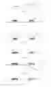
BRIEF DESCRIPTION OF THE DRAWINGS
FIG. 1 illustrates a first step in the process showing to components of two different vertical dimensions before their placement on an adhesive substrate.
FIG. 2 illustrates a further step in the process wherein adhesive is placed on top of the components after they have been placed on the adhesive substrate.
FIG. 3 illustrates a further step in the process wherein a component fixture having aligned compartments is arranged above the components with adhesive already placed on their top surfaces.
FIG. 4 illustrates a further step in the process where the component fixture has been pressed against the adhesive substrate and wherein excess adhesive has been extruded through a vent hole or aperture from the compartments.
FIG. 5 illustrates a further step of the process showing the removal of the adhesive substrate.
FIG. 6 illustrates a completed part after the removal of the adhesive substrate.
DETAILED DESCRIPTION OF THE PREFERRED EMBODIMENTS
Referring to FIG. 1, a pair of components 20 and 30 of different vertical heights are shown floating above and adhesive substrate 10 prior to being placed upon the adhesive substrate 10. The adhesive substrate may be supported on a flat surface as is conventional, and may itself be a laminate of one or more layers of, for example metal foil 12, see FIG. 2, and an adhesive layer 10. The adhesive itself is preferably selected from a group consisting of low tack, pressure sensitive acrylic and thermal release films or tapes for hard substrate such as Nitto Denko material NWS-Y5V/NWS-TS322F
Each of the components, which may have different vertical heights (and lengths and widths), are package integrated circuits having formed thereon electrical contacts 22 and 32 that will physically contact the adhesive substrate 10. While illustrated in the figure as contacts spaced about the bottom surfaces of the components 20 and 30, the contacts could be of the gullwing, J-leaded or other lead shape variety as illustrated in the aforementioned U.S. Pat. No. 7,926,173. See e.g. FIGS. 8 and 9 of U.S. '173, and the gullwing components 802.
The adhesive may be provided with tooling holes 14 that may be used to provide apertures for tools to better align the adhesive substrate and the tooling, not shown, that physically places the components 20 and 30 on the adhesive substrate 10.
Referring to FIG. 2, the figure illustrates the components 20 and 30 after they are accurately placed on the adhesive substrate 10. In this step, a metal layer 12 may be applied to the adhesive substrate 10. In subsequent processing, provided the surfaces of the carrier 70 are non conductive this metal layer 12 may be patterned the form electrical traces to the contacts 22 and 32 of the components 20 and 30 as illustrated either in U.S. '173, which shows connections through vias through the adhesive substrate or in co-pending application Ser. No. 12/170,426 wherein the electrical connection is due to the adhesive itself being anisotropically conductive such as 3M 5363 an anisotropic conductive film which is comprised of a mixture of epoxy and acrylic resins and a curative in combination with conductive particles dispersed within the mixture so as to be conductive in the Z or vertical axis and insulating in the X and Y directions
Alternatively to applying the metal foil layer 12 in step two (FIG. 2), the adhesive substrate 10 may itself comprise a laminate structure consisting of the adhesive substrate 10 and the metal foil 12.
Again referring to FIG. 2, an adhesive is applied to the top surfaces of components 20 and 30, resulting in a piled layer of adhesive 42 and 40 respectively. While the amount of the adhesive in a pile might be within defined ranges, as known in the art, the amount can vary from sample to sample. For this reason, both the vertical height of the components 20 and 30 and the amount of adhesive in piles 42 and 40 may vary within tolerance ranges.
Referring to FIG. 3, a component support fixture 70 having compartments 50 and 52 is shown arranged above components 30 and 20 prior to the fixture being lowered into place. As illustrated in the figure, each of the compartments 50 and 52 additionally has a vent hole or aperture 60 and 62. The purpose of a vent hole or aperture is to allow venting both of air and of excess adhesive from the respective compartments 50 and 52 as the component support fixture 70 is lowered into place about components 30 and 20 and is pressed into abutment (not shown) with the adhesive substrate 10 as illustrated in FIG. 4.
As illustrated in FIG. 4, the size of the compartments 50 and 52 is chosen such that they can accommodate components of all sizes in the both the vertical and horizontal ranges and allow space both above and to the sides of the components 30 and 20 within the compartment 50 and 52. The size is further chosen such that the pile of adhesive 40 or 42 is squeezed about the components 30 and 20 within the compartments 50 and 52. When the size of the components versus the size of the compartments is such that there is insufficient space remaining within the compartments for the excess adhesive, the vent hole or aperture provides for the extrusion of adhesive 40 and 42 through vent holes or apertures 60 and 62, as the component support fixture 70 is pressed down until its bottom surface 72 is pressed into contact with the adhesive substrate 10.
Referring to FIG. 4, the figure shows the component support fixture 70 in place, contacting the adhesive layer 10 via its lower surface 72. As well, the piles of adhesive 40 and 42 have been squeezed into the spaces 54 and 56 between the components 30 and 20 and the compartments 50 and 52. At this point, the adhesive could be allowed to be cured, at which time electrical contacts could be made according to the aforementioned co-pending applications to provide via connections to the contacts 32, 22, or traces by etching the metal foil 12 as provided in Ser. No. 12/170,426.
Referring to FIG. 5, in an alternative embodiment, the adhesive 10 could be removed by for example chemical stripping or peeling it from the completed component support fixture/component, as shown in the figure. To facilitate removal the material could be a heat releasable material as mentioned earlier. This is preferentially accomplished by providing the adhesive with a layer 12, which could be the metal foil layer 12 as described above, but it also could be any other suitable layer that would support the adhesive layer during the previous processing steps. Such a suitable layer could be any of various stable polymer films which could serve as a carrier for the adhesive including polyester, polyethelyne napthalate or polyimide.
Referring to FIG. 6, the completed part is shown after the adhesive layer 10 has been removed. This part may be used in subsequent manufacturing steps where the components 30 and 20 could be further processed using an Occam process or otherwise to provide electrical connections to other elements on a circuit board. Also, it is intended that the adhesive 40 or 42 be chosen such that the component support fixture 70 might be removed entirely after such subsequent processing.
For this purpose, it is understood that the component support fixture 70 can be made of any material for the purpose sense if invites only temporary manufacturing support for the components 30 and 20. If however component support fixture 70 is intended to be permanent, it could be made of a material that is insulating or conductive depending on the purpose for the support, and it further could be made out of a material having a high thermal conductivity, such as aluminum. Examples of materials in the latter category include epoxy glass laminates or molded thermoplastic materials such as PEEK.
The description of the various embodiments above are not to be taken as a limitation on the scope of the invention. Variations of materials and structures and sequence of steps to achieve the overall objective of providing a component support fixture with vent holes or apertures either as a partial step in an Occam process, or as a completed structure in an Occam process, or other process, is within the scope of the present invention.
Claims
I claim:1. A process comprising:
placing components on an adhesive film;
coating the components with an adhesive;
placing a component support fixture over the components and pressed against the adhesive film, component support fixture comprising compartments of a slightly larger size then the components, the component support fixture including a vent aperture sized for both venting air from the compartment and extruding excess adhesive;
whereby a component surface is aligned with a surface of the component support fixture and further whereby excess adhesive is extruded through the vent.
2. The process according to claim one wherein the adhesive coating the components is compatible with the adhesive of the adhesive film.
3. The process according to claim one wherein the compartment size is large enough for the adhesive coating the component to be squeezed in to space between the component and the compartment.
4. The process according to claim three wherein the space between the component and the compartment includes spaces surrounding the sides of the component.
5. The process according to claim one wherein the adhesive of the foil comprises an anisotropically conductive material.
6. The process according to claim five wherein the foil is electrically conductive in the anisotropic direction of low resistance is between the component and the electrically conductive foil.
7. The process according to claim one wherein the adhesive film comprises tooling holes, whereby tools may be used to locate accurate placement of the components on the adhesive film.
8. The process according to claim one wherein the component support fixture comprises a machined surface for supporting the adhesive film.
9. The process according to claim nine wherein the component support fixture comprises a machine lid.
10. The process according to claim nine wherein the component support fixture comprises a molded lid.
Images & Drawings included:

Sources:
- United States Patent and Trademark Office - verify current appl. status at the USPTO↗
Recent applications in this class:
- » 20250240894 2025-07-24
DISPLAY DEVICE - » 20250227852 2025-07-10
ELECTRONIC DEVICE COMPRISING SOLDER WALL - » 20250159814 2025-05-15
FLEXIBLE CIRCUIT BOARD, DISPLAY MODULE, AND ELECTRONIC DEVICE - » 20250151201 2025-05-08
FLEXIBLE AND STRETCHABLE STRUCTURES - » 20250133660 2025-04-24
RESTRICTING DEVICE FOR FLEXIBLE WIRING BOARD AND DISPLAY DEVICE USING THE RESTRICTING DEVICE - » 20250098073 2025-03-20
DYNAMIC FLEXIBLE CIRCUITS - » 20250071908 2025-02-27
DISPLAY MODULE AND DISPLAY DEVICE - » 20250063669 2025-02-20
Conformal Wearable Battery - » 20250048559 2025-02-06
DRAPABLE, FLEXIBLE CIRCUITRY LAYERS AND METHODS THEREFOR - » 20250048558 2025-02-06
DISPLAY DEVICE AND METHOD FOR PRODUCING SAME
Recent applications for this Assignee:
- » 20120211265 2012-08-23
Flexible circuit assembly without solder - » 20120077293 2012-03-29
Light-Emitting Diode Package Assembly - » 20120006589 2012-01-12
Electronic assemblies without solder and methods for their manufacture - » 20110199740 2011-08-18
Monolithic molded flexible electronic assemblies without solder and methods for their manufacture - » 20110182042 2011-07-28
Electronic Assemblies without Solder and Methods for their Manufacture - » 20110127080 2011-06-02
Electronic Assemblies without Solder and Methods for their Manufacture - » 20100096166 2010-04-22
Flexible circuit assemblies without solder and methods for their manufacture - » 20090278139 2009-11-12
Light emitting diode package assembly - » 20090277677 2009-11-12
Electronic Assemblies without Solder and Method for their Design, Prototyping, and Manufacture - » 20090237901 2009-09-24
Monolithic molded flexible electronic assemblies without solder and methods for their manufacture