Laminated transferable interconnect for microelectronic package
US20120139100A1
2012-06-07
12/959,549
2010-12-03
✅ Patent granted
US 8,969,176 B2
2015-03-03
-
-
James Mitchell
Daly, Crowley, Mofford & Durkee, LLP
2032-05-04
Abstract:
A package for a plurality of semiconductor devices having: an electrical interconnect structure, comprising: an electrical interconnect structure; and an active device structure, comprising the plurality of semiconductor devices on an active device substrate. The electrical interconnect structure is bonded to the active device structure and the electrical interconnect structure provides electrical interconnection among the semiconductor devices.
Inventors:
- William J. Davis 9 🇺🇸 Hollis, NH, United States
- Ward G. Fillmore 7 🇺🇸 Hudson, MA, United States
Assignee:
- RAYTHEON COMPANY 5,596 🇺🇸 Waltham, MA, United States
Applicant:
Interested in similar patents?
Get notified when new applications in this technology area are published.
Classification:
H01L21/683 IPC
Processes or apparatus adapted for the manufacture or treatment of semiconductor or solid state devices or of parts thereof; Apparatus specially adapted for handling semiconductor or electric solid state devices during manufacture or treatment thereof; Apparatus specially adapted for handling wafers during manufacture or treatment of semiconductor or electric solid state devices or components ; Apparatus not specifically provided for elsewhere for supporting or gripping
H01L2924/00013 » CPC further
Indexing scheme for arrangements or methods for connecting or disconnecting semiconductor or solid-state bodies as covered by; Technical content checked by a classifier Fully indexed content
B81C1/00 IPC
Manufacture or treatment of devices or systems in or on a substrate
H01L23/544 » CPC further
Details of semiconductor or other solid state devices Marks applied to semiconductor devices , e.g. registration marks,
H01L2224/13099 » CPC further
Indexing scheme for arrangements for connecting or disconnecting semiconductor or solid-state bodies and methods related thereto as covered by; Means for bonding being attached to, or being formed on, the surface to be connected, e.g. chip-to-package, die-attach, "first-level" interconnects; Manufacturing methods related thereto; Bump connectors; Manufacturing methods related thereto; Structure, shape, material or disposition of the bump connectors prior to the connecting process of an individual bump connector; Core members of the bump connector Material
H01L2224/13599 » CPC further
Indexing scheme for arrangements for connecting or disconnecting semiconductor or solid-state bodies and methods related thereto as covered by; Means for bonding being attached to, or being formed on, the surface to be connected, e.g. chip-to-package, die-attach, "first-level" interconnects; Manufacturing methods related thereto; Bump connectors; Manufacturing methods related thereto; Structure, shape, material or disposition of the bump connectors prior to the connecting process of an individual bump connector; Coating Material
H01L2224/05599 » CPC further
Indexing scheme for arrangements for connecting or disconnecting semiconductor or solid-state bodies and methods related thereto as covered by; Means for bonding being attached to, or being formed on, the surface to be connected, e.g. chip-to-package, die-attach, "first-level" interconnects; Manufacturing methods related thereto; Bonding areas; Manufacturing methods related thereto; Structure, shape, material or disposition of the bonding areas prior to the connecting process of an individual bonding area; External layer Material
H01L2224/05099 » CPC further
Indexing scheme for arrangements for connecting or disconnecting semiconductor or solid-state bodies and methods related thereto as covered by; Means for bonding being attached to, or being formed on, the surface to be connected, e.g. chip-to-package, die-attach, "first-level" interconnects; Manufacturing methods related thereto; Bonding areas; Manufacturing methods related thereto; Structure, shape, material or disposition of the bonding areas prior to the connecting process of an individual bonding area; Internal layers Material
H01L2224/29099 » CPC further
Indexing scheme for arrangements for connecting or disconnecting semiconductor or solid-state bodies and methods related thereto as covered by; Means for bonding being attached to, or being formed on, the surface to be connected, e.g. chip-to-package, die-attach, "first-level" interconnects; Manufacturing methods related thereto; Layer connectors, e.g. plate connectors, solder or adhesive layers; Manufacturing methods related thereto; Structure, shape, material or disposition of the layer connectors prior to the connecting process of an individual layer connector; Core members of the layer connector Material
H01L2224/29599 » CPC further
Indexing scheme for arrangements for connecting or disconnecting semiconductor or solid-state bodies and methods related thereto as covered by; Means for bonding being attached to, or being formed on, the surface to be connected, e.g. chip-to-package, die-attach, "first-level" interconnects; Manufacturing methods related thereto; Layer connectors, e.g. plate connectors, solder or adhesive layers; Manufacturing methods related thereto; Structure, shape, material or disposition of the layer connectors prior to the connecting process of an individual layer connector; Coating Material
H01L2924/00 » CPC further
Indexing scheme for arrangements or methods for connecting or disconnecting semiconductor or solid-state bodies as covered by
H01L23/48 IPC
Details of semiconductor or other solid state devices Arrangements for conducting electric current to or from the solid state body in operation, e.g. leads, terminal arrangements ; Selection of materials therefor
H01L21/50 IPC
Processes or apparatus adapted for the manufacture or treatment of semiconductor or solid state devices or of parts thereof; Manufacture or treatment of semiconductor devices or of parts thereof the devices having at least one potential-jump barrier or surface barrier, e.g. PN junction, depletion layer or carrier concentration layer Assembly of semiconductor devices using processes or apparatus not provided for in a single one of the subgroups - , e.g. sealing of a cap to a base of a container
B81C1/00301 » CPC main
Manufacture or treatment of devices or systems in or on a substrate for manufacturing microsystems; Processes for packaging MEMS devices Connecting electric signal lines from the MEMS device with external electrical signal lines, e.g. through vias
H01L21/6835 » CPC further
Processes or apparatus adapted for the manufacture or treatment of semiconductor or solid state devices or of parts thereof; Apparatus specially adapted for handling semiconductor or electric solid state devices during manufacture or treatment thereof; Apparatus specially adapted for handling wafers during manufacture or treatment of semiconductor or electric solid state devices or components ; Apparatus not specifically provided for elsewhere for supporting or gripping using temporarily an auxiliary support
H01L2221/68359 » CPC further
Processes or apparatus adapted for the manufacture or treatment of semiconductor or solid state devices or of parts thereof covered by; Apparatus for handling semiconductor or electric solid state devices during manufacture or treatment thereof; Apparatus for handling wafers during manufacture or treatment of semiconductor or electric solid state devices or components; Apparatus not specifically provided for elsewhere for supporting or gripping using temporarily an auxiliary support used as a support during manufacture of interconnect decals or build up layers
H01L2221/68363 » CPC further
Processes or apparatus adapted for the manufacture or treatment of semiconductor or solid state devices or of parts thereof covered by; Apparatus for handling semiconductor or electric solid state devices during manufacture or treatment thereof; Apparatus for handling wafers during manufacture or treatment of semiconductor or electric solid state devices or components; Apparatus not specifically provided for elsewhere for supporting or gripping using temporarily an auxiliary support used in a transfer process involving transfer directly from an origin substrate to a target substrate without use of an intermediate handle substrate
H01L2221/68381 » CPC further
Processes or apparatus adapted for the manufacture or treatment of semiconductor or solid state devices or of parts thereof covered by; Apparatus for handling semiconductor or electric solid state devices during manufacture or treatment thereof; Apparatus for handling wafers during manufacture or treatment of semiconductor or electric solid state devices or components; Apparatus not specifically provided for elsewhere for supporting or gripping using temporarily an auxiliary support Details of chemical or physical process used for separating the auxiliary support from a device or wafer
H01L2223/54426 » CPC further
Details relating to semiconductor or other solid state devices covered by the group; Marks applied to semiconductor devices or parts for alignment
B81B2207/092 » CPC further
Microstructural systems or auxiliary parts thereof; Packages; Arrangements for connecting external electrical signals to mechanical structures inside the package Buried interconnects in the substrate or in the lid
B81B2207/095 » CPC further
Microstructural systems or auxiliary parts thereof; Packages; Arrangements for connecting external electrical signals to mechanical structures inside the package; Feed-through, via through the lid
H01L2924/0002 » CPC further
Indexing scheme for arrangements or methods for connecting or disconnecting semiconductor or solid-state bodies as covered by; Technical content checked by a classifier Not covered by any one of groups , and
H01L21/44 IPC
Processes or apparatus adapted for the manufacture or treatment of semiconductor or solid state devices or of parts thereof; Manufacture or treatment of semiconductor devices or of parts thereof the devices having at least one potential-jump barrier or surface barrier, e.g. PN junction, depletion layer or carrier concentration layer the devices having semiconductor bodies not provided for in groups, , , and with or without impurities, e.g. doping materials Manufacture of electrodes on semiconductor bodies using processes or apparatus not provided for in groups -
H01L21/00 IPC
Processes or apparatus adapted for the manufacture or treatment of semiconductor or solid state devices or of parts thereof
Description
TECHNICAL FIELD
This invention relates generally to methods for packaging (i.e., encapsulating) semiconductors and more particularly to methods for packaging semiconductors at a wafer level (i.e., wafer-level packaging).
BACKGROUND AND SUMMARY
As is known in the art, traditionally in the microelectronics industry, electrical devices are fabricated on wafers and then diced into individual chips. The bare chips would then get assembled with other components into a package for environmental and mechanical protection. In commercial applications, the chips were generally assembled into plastic packages. In military applications, where electronics are generally exposed to harsher environments, the parts are generally housed in a hermetic module. Such packages or modules would then be further assembled unto circuit boards and systems. However, as electronic systems advance, there is a need to increase functionality while decreasing the size and cost of components and sub-systems.
In accordance with the present disclosure, a package for a plurality of semiconductor devices is provided comprising: an electrical interconnect structure; and an active device structure, comprising the plurality of semiconductor devices on an active device substrate. The electrical interconnect structure is bonded to the active device structure and the electrical interconnect provides electrical interconnection among the semiconductor devices.
In one embodiment, a method is provided for packaging a plurality of semiconductor devices. The method includes: forming an electrical interconnect structure, comprising: a support substrate; a release layer on the support substrate; and a patterned electrical interconnect over the release layer. An active device structure is formed, comprising: forming the plurality of semiconductor devices on an active device substrate. The electrical interconnect structure is bonded to the active device structure.
In one embodiment, electrical interconnections are made between the active devices and the patterned electrical interconnect; and wherein the support substrate is removed from the bonded electrical interconnect structure and the active device structure.
In one embodiment, the support substrate is removed from the bonded electrical interconnect structure and the active device structure.
In one embodiment, a method is provided for packaging a plurality of semiconductor devices. The method includes: forming an electrical interconnect structure, comprising: a support substrate; a release layer on the support substrate; and a patterned electrical interconnect over the release layer; forming an active device structure, comprising: forming the plurality of semiconductor devices on an active device substrate; bonding the electrical interconnect structure to the active device structure;
In one embodiment, the method includes making electrical interconnections between the active devices and the patterned electrical interconnect structure; and; removing the support substrate from the bonded electrical interconnect structure and the active device structure.
In one embodiment, the removing comprises chemically removing the release layer.
In one embodiment, the removing comprises dissolving the release layer.
In one embodiment, the electrical interconnect structure is a laminated structure comprising a plurality of patterned electrical interconnects, each one of the of patterned electrical interconnects being separated by a dielectric layer.
In one embodiment, a method is provided for packaging a plurality of semiconductor devices. The method includes: forming an electrical interconnect structure, such interconnect structure comprising: a support substrate; a release layer on the support substrate; and a patterned electrical interconnect over the release layer; forming an active device structure, comprising: forming the plurality of semiconductor devices in the surface portion of the surface of the semiconductor wafer; bonding the electrical interconnect structure to the active device structure including making electrical interconnections between the active devices and the patterned electrical interconnect; and removing the support substrate from the bonded electrical interconnect structure and the active device structure comprising chemically removing the release layer.
In one embodiment, the electrical interconnect structure is a laminated structure comprising a plurality of patterned electrical interconnects, each one of the of patterned electrical interconnects being separated by a dielectric layer.
The details of one or more embodiments of the disclosure are set forth in the accompanying drawings and the description below. Other features, objects, and advantages of the disclosure will be apparent from the description and drawings, and from the claims.
DESCRIPTION OF DRAWINGS
FIGS. 1A through 1L are simplified cross-sectional views showing an electrical interconnect structure at various stages in the fabrication thereof;
FIGS. 2A through 2D are simplified cross-sectional views showing an active device structure at various stages in the fabrication thereof;
FIGS. 3A through 3D are simplified cross-sectional views showing the bonding of the an electrical interconnect structure and the active device structure at various stages thereof.
Like reference symbols in the various drawings indicate like elements.
DETAILED DESCRIPTION
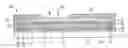
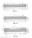
Referring now to FIGS. 1A through 1L, an electrical interconnect structure 10 (FIG. 1L) is formed. More particularly, a low cost transparent substrate 12 (FIG. 1A) is provided, such as glass or silicon having a thickness in the order of, for example, 500 microns. A release layer 14 (FIG. 1B) material is applied to coat the upper surface of the substrate 12. Next, a top dielectric layer 16 (FIG. 1C) of here, for example, BCB is applied to the surface of the release layer 14. Next, a seed layer 18 (FIG. 1D) of here for example, gold, is vacuum deposited or sputter deposited over the top dielectric layer 16 here, for example, to a thickness of 1000 to 2000 Angstroms. Next, a photoresist layer 20 (FIG. 1E) is coated over the seed layer 18 and photo lithographically masked and etched to form a predetermined pattern of windows (not shown) to expose regions 21 of the seed layer 18 where electrical interconnects 23 and alignment targets 25 are to be formed. Next, electroplating of a conductive layer 22 (FIG. 1F) here, for example, gold is performed on the exposed regions 21 of the seed layer 18 to build up the thickness of the desired electrical interconnects and passive elements, to be described. Here, for example the thickness of the interconnects and passive elements is in the order of 4-5 microns electrical interconnects.
Next, the photoresist layer 20 is removed using any conventional process (FIG. 1G) followed by removal of the underlying seed layer 18 using for example potassium cyanide (FIG. 1H). Next, a second dielectric layer 30, here for example BCB, is coated over the resulting structure, as shown in FIG. 1I. Next, a second seed layer 32 (FIG. 1J) of for example gold is deposited over the second dielectric layer 30. Next, a second photoresist layer 34 (FIG. 1J) is coated over the seed layer 32 and patterned using conventional photolithographic processing to having windows formed therein to expose predetermined selected regions 36 of the second seed layer 32, as shown. The pattern in the second photoresist layer 34 is selected to form an upper level of electrical interconnects, passive components such as transmission lines, impedance matching structures, inductors to be described. The selected exposed regions of the second seed layer 32 are electroplated with a conductive material 38, for example gold, to build up the thickness of second level of layer of electrical interconnects to the desired second level of electrical interconnects, passive components such as transmission lines, impedance matching structures, inductors to be described. Here, for example the thickness of the interconnect layer 38 is in the order of 4-5 microns. Thus, an electrical interconnect is formed by layers 20, 32 and 38 as shown in FIG. 1J.
Next, the second photoresist layer 34 is selectively removed and the underlying portions of the second seed layer 32 are etched away (it being noted that the portions of the seed layer 32 under layer 38 remain) followed by removal of the dielectric layer 30 (FIG. 1K). Next, a third, top, dielectric layer 40 (FIG. 1K), here for example, BCB is coated over the resulting structure as shown in FIG. 1K. Next, an uncured glue layer 42, here, for example, BCB is coated over the top dielectric layer 40 and over layer 38, and then patterned with a window 44, as shown in FIG. 1L to complete the interconnect structure 10.
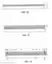
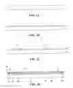
Referring to FIGS. 2A-2D, an active device sub-assembly or structure 50 (FIG. 2D) is formed. More particularly, a high cost active substrate 52 (FIG. 2A), for example a semiconductor substrate 52, for example, GaN, is provided. A semiconductor epitaxial layer 54 (FIG. 2B), here GaN, for example, is deposited or grown over the active substrate 52. Next, active devices 56 such as field effect transistors and passive components such as transmission lines, impedance matching structures, inductors or capacitors, for example, are formed in the surface of the structure, as shown in FIG. 2C). Next, electrically conductive contact pads 58 and alignment structures 60, here for example, gold, are formed over the structure using any conventional photolithographic deposition processes. Next, a dielectric bond layer 62, here for example BCB, is applied over the active device structured 50, as shown in FIG. 2D.
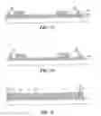
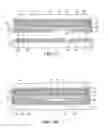
Having formed the interconnect sub-assembly structure 10 and the active device sub-assembly or structure 50, the two structures 10, 50 are aligned with the alignment marks (FIG. 3A) and then bonded together (FIG. 3B), here, for example, by thermo-compression bonding. Next, the release layer 14 is removed, here by using a suitable chemical such as for example sodium borate, potassium borate or other aqueous developer thereby removing the low cost transparent substrate thereby removing the substrate low cost transparent 12 (FIG. 3C). Next, the bonded structure is processed using conventional photolithography and plating to form electrical interconnects between the interconnect sub-assembly structure and the active device sub-assembly or structure, as shown in FIG. 3D. More particularly, a vias are formed, here by, for example, layer ablation or chemical etching, through the layer 40 and processed in any convectional manner to form an electrical interconnects 60a, 60b thereby electrically interconnecting passive conductor 20, conductor 32 and conductor 38, as indicated and active elements 56a, 56b, here for example individual FETS or MEMs, or SAW devices. It is noted that there is an air gap 70 over the individual active elements 56a, 56b.
A number of embodiments of the disclosure have been described. Nevertheless, it will be understood that various modifications may be made without departing from the spirit and scope of the disclosure. Accordingly, other embodiments are within the scope of the following claims.
Claims
What is claimed is:1. A package for a plurality of semiconductor devices, comprising:
an electrical interconnect structure;
an active device structure, comprising the plurality of semiconductor devices on an active device substrate;
wherein the electrical interconnect structure is bonded to the active device structure and the electrical interconnect structure provides electrical interconnection among the semiconductor devices.
2. A method for packaging a plurality of semiconductor devices, comprising:
forming an electrical interconnect structure, comprising:
a support substrate;
a release layer on the support substrate; and
a patterned electrical interconnect structure over the release layer;
forming an active device structure, comprising:
forming the plurality of semiconductor devices on an active device substrate;
bonding the electrical interconnect structure to the active device structure; and
removing the support substrate from the bonded electrical interconnect structure and the active device structure.
3. The method recited in claim 2 including making electrical interconnections between the active devices and the patterned electrical interconnect structure.
4. The method recited in claim 3 wherein the removing comprises chemically removing the release layer.
5. The method recited in claim 3 wherein the removing comprises dissolving the release layer.
6. The method recited in claim 3 wherein the electrical interconnect structure is a laminated structure comprising a plurality of patterned electrical interconnect structures, each one of the of patterned electrical interconnects being separated by a dielectric layer.
7. A method for packaging a plurality of semiconductor devices formed in a surface portion of a semiconductor wafer, such method comprising:
forming an electrical interconnect structure, such interconnect structure comprising:
a support substrate;
a release layer on the support substrate; and
a patterned electrical interconnect structure over the release layer;
forming an active device structure, comprising:
forming the plurality of semiconductor devices in the surface portion of the surface of the semiconductor wafer;
bonding the electrical interconnect structure to the active device structure including making electrical interconnections between the active devices and the patterned electrical interconnect structure;
removing the support substrate from the bonded electrical interconnect structure and the active device structure comprising chemically removing the release layer.
8. The method recited in claim 7 wherein the electrical interconnect structure is a laminated structure comprising a plurality of patterned electrical interconnects, each one of the patterned electrical interconnects being separated by a dielectric layer.
Images & Drawings included:
Sources:
- United States Patent and Trademark Office - verify current appl. status at the USPTO↗
Recent applications in this class:
- » 20240327206 2024-10-03
METHODS FOR FABRICATION OF MEMS DEVICE - » 20240317580 2024-09-26
MEMS DEVICE AND MANUFACTURING METHOD OF MEMS DEVICE - » 20240116753 2024-04-11
METHOD FOR SEALING A MEMS DEVICE AND A SEALED MEMS DEVICE - » 20240116752 2024-04-11
PACKAGED CAVITY STRUCTURE AND MANUFACTURING METHOD THEREOF - » 20210371273 2021-12-02
RESONANCE DEVICE AND RESONANCE DEVICE MANUFACTURING METHOD - » 20210309512 2021-10-07
Method for manufacturing a MEMS sensor - » 20200283292 2020-09-10
MEMS structure including a cap with a via - » 20200180948 2020-06-11
Method of manufacturing semiconductor device and semiconductor device - » 20200062587 2020-02-27
Semiconductor arrangement and formation thereof - » 20190284044 2019-09-19
Semiconductor device and manufacture thereof
Recent applications for this Assignee:
- » 20250167415 2025-05-22
ENHANCED BROADBAND RING RESONATOR FOR IMPROVED SPECTRAL SUPPRESSION - » 20250145355 2025-05-08
INTEGRATED CABLE PACKAGING, DEPLOYMENT AND STRUMMING MITIGATION SYSTEM - » 20250118501 2025-04-10
MICRO-ELECTROMECHANICAL SYSTEMS SWITCH WITH BEAM MOVEMENT ORTHOGONAL TO FORCE - » 20250116997 2025-04-10
PRODUCT IDENTIFICATION AND TRACKING SYSTEMS AND METHODS - » 20250116851 2025-04-10
REIMAGING LENS ASSEMBLY WITH ANGLED OPTIC - » 20250107006 2025-03-27
RF COVER LAYER - » 20250067792 2025-02-27
DEVICE FOR AND METHOD OF FREQUENCY TESTING PRINTED CIRCUIT BOARD UNDER THERMAL STRESS - » 20250062543 2025-02-20
CONFORMAL WAVEFRONT TRANSFORMER AND METHOD OF MAKING - » 20250035410 2025-01-30
TACTICAL HIGH POWER MICROWAVE ANTENNA PEDESTAL - » 20250027811 2025-01-23
ANTI-BLOOMING BUFFERED DIRECT INJECTION PIXELS