SILTRONIC AG
Munich
Germany
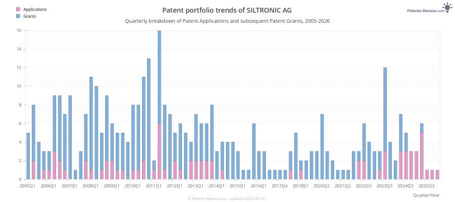
360
2025-09-11
303
2026-05-19
Top Inventors for applications by SILTRONIC AG
These are the the leading inventors for applications assigned to SILTRONIC AG:
- Juergen Schwandner 27 Garching, Germany
- Georg Pietsch 26 Burghausen, Germany
- Reinhold Wahlich 21 Tittmoning, Germany
- Reinhard SCHAUER 17 Laufen, Germany
- Thomas Buschhardt 17 Burghausen, Germany
- Wilfried von Ammon 16 Hochburg, Austria
- Wilfried von Ammon 15 Hochburg/Ach, Austria
- Katsuhiko Nakai 15 Yamaguchi, Japan
- Brian Murphy 14 Pfarrkirchen, Germany
- Andreas Huber 14 Garching, Germany
- Martin WEBER 14 Kastl, Germany
- Peter Wiesner 14 Reut, Germany
- Teruo Haibara 13 Hikari, Japan
- Michael Kerstan 13 Burghausen, Germany
- Andreas Sattler 12 Trostberg, Germany
- Timo Mueller 11 Burghausen, Germany
- Diego Feijoo 11 Burghausen, Germany
- Norbert WERNER 11 Tengling, Germany
- Georg Brenninger 11 Oberbergkirchen, Germany
- Katsuhiko Nakai 10 Hikari, Japan
- Guenter Schwab 10 Neuoetting, Germany
- Christian HAGER 10 Kastl, Germany
- Yoshihiro Mori 10 Shunan, Japan
- Peter Storck 10 Burghausen, Germany
- Klaus Roettger 10 Bachmehring, Germany
- Roland Koppert 9 Triftern, Germany
- Anton Huber 9 Burghausen, Germany
- Walter HEUWIESER 8 Stammham, Germany
- Joerg HABERECHT 8 Freiberg, Germany
- Ludwig Altmannshofer 7 Massing, Germany
- Karl MANGELBERGER 7 Ach, Austria
- Georg Raming 7 Tann, Germany
- Leszek Mistur 7 Burghausen, Germany
- Alexander Heilmaier 7 Haiming, Germany
- Herbert Schmidt 7 Halsbach, Germany
- Gudrun Kissinger 6 Lebus, Germany
- Atsushi Ikari 6 Yamaguchi, Japan
- Etsuko Kubo 6 Hikari, Japan
- Thomas SCHROECK 6 Kastl, Germany
- Masashi Uchibe 6 Hikari, Japan
- Friedrich Passek 6 Adlkofen, Germany
- Alfred MILLER 6 Emmerting, Germany
- Robert Kreuzeder 6 Wurmannsquick, Germany
- Teruo Haibara 5 Yamaguchi, Japan
- Stefan WELSCH 5 Polling, Germany
- Wolfgang Gmach 5 Emmerting, Germany
- Clemens Zapilko 5 Burghausen, Germany
- Joachim Junge 5 Burghausen, Germany
- Masashi Uchibe 5 Izumo, Japan
- Michael GEHMLICH 5 Weissenborn, Germany
- Sarad Bahadur Thapa 5 Burghausen, Germany
- Helmut Schwenk 5 Burghausen, Germany
- Etsuko Kubo 5 Yokkaichi, Japan
- Robert Hoelzl 4 Postmuenster, Germany
- Christof WEBER 4 Burghausen, Germany
- Hans Oelkrug 4 Tittmoning, Germany
- Masamichi Ohkubo 4 Yamaguchi, Japan
- Gerhard Heier 4 Burghausen, Germany
- Markus Blietz 4 Tittmoning, Germany
- Michael SKROBANEK 4 Freiberg, Germany
- Robert Vorbuchner 4 Burghausen, Germany
- Maximilian Stadler 4 Haiming, Germany
- Ulrich Lambert 4 Emmerting, Germany
- Walter HAECKL 4 Zeilarn, Germany
- Carl FRINTERT 4 Muehldorf am Inn, Germany
- Dieter Knerer 4 Burghausen, Germany
- SILTRONIC AG 4 Munich, Germany
- Vladimir Dutschke 4 Lengefeld, Germany
- Thomas SCHROEDER 4 Berlin, Germany
- Martin VORDERWESTNER 4 Unterreit, Germany
- Erich Daub 4 Emmerting, Germany
- Hannes HECHT 4 Burghausen, Germany
- Dirk Dantz 4 Koenigslutter am Elm, Germany
- Peter Storck 4 Mehring, Germany
- Hideo Kato 3 Hikari, Japan
- Juergen Vetterhoeffer 3 Burghausen, Germany
- Rudiger Schmolke 3 Burghausen, Germany
- Robert Weiss 3 Winhoering, Germany
- Sebastian Geissler 3 Brand-Erbisdorf, Germany
- Shigeki Nishimura 3 Yamaguchi, Japan
- Frank LAUBE 3 Burghausen, Germany
- Axel BEYER 3 Munich, Germany
- Ludwig LAMPRECHT 3 Truchtlaching, Germany
- Andrej LENZ 3 Tittmoning, Germany
- Thomas STETTNER 3 Waging am See, Germany
- Alexander VOLLKOPF 3 Burghausen, Germany
- Axel BEYER 3 Burghausen, Germany
- Werner Schachinger 3 Simbach, Germany
- Michael Boy 3 Waging am See, Germany
- Wolfgang Siebert 3 Mehring, Germany
- Joerg Moser 3 Unterneukirchen, Germany
- Patrick MOOS 3 Pleiskirchen, Germany
- Shinichi Kyufu 3 Hikari, Japan
- Guido Wenski 3 Burghausen, Germany
- Torsten Olbrich 3 Dresden, Germany
- Dirk Zemke 3 Marktl, Germany
- Rupert Krautbauer 3 Portland, OR United States
- Janis Virbulis 3 Burghausen, Germany
- Masayuki Fukuda 3 Yamaguchi, Japan
- Axel Beyer 3 Seoul, South Korea
Recent patent applications by SILTRONIC AG
SILTRONIC AG based in Munich, DE has been assigned the rights to these inventions. The list includes both Pending Applications and Patent Grants:
US20250283249A1
Chemistry; metallurgySEMICONDUCTOR WAFER MADE OF SINGLE-CRYSTAL SILICON AND PROCESS FOR THE PRODUCTION THEREOF
#2 | 2025-06-19 ✅ Patent 12,635,442 granted on 2026-05-19US20250201547A1
ElectricityMETHOD FOR CLEANING A SEMICONDUCTOR WAFER
#3 | 2024-09-19 ✅ Patent 12,637,786 granted on 2026-05-26US20240309552A1
Chemistry; metallurgyMETHOD FOR PRODUCING A GALLIUM OXIDE LAYER ON A SUBSTRATE
#4 | 2024-07-25 ✅ Patent 12,479,128 granted on 2025-11-25US20240246260A1
Performing operations; transportingMETHOD FOR PRODUCING SEMICONDUCTOR WAFERS USING A WIRE SAW, WIRE SAW, AND SEMICONDUCTOR WAFERS MADE OF MONOCRYSTALLINE SILICON
#5 | 2024-05-30 ✅ Patent 12,308,267 granted on 2025-05-20US20240178026A1
ElectricityApparatus for transporting semiconductor wafers
#6 | 2024-05-09 ✅ Patent 12,503,791 granted on 2025-12-23US20240150932A1
Chemistry; metallurgyMETHOD OF PRODUCING EPITAXIAL LAYER WAFERS IN A CHAMBER OF A DEPOSITION REACTOR
#7 | 2024-05-09 ✅ Patent 12,553,145 granted on 2026-02-17US20240150927A1
Chemistry; metallurgyAPPARATUS AND METHOD FOR PRODUCING A DOPED MONOCRYSTALLINE ROD MADE OF SILICON
#8 | 2024-04-25 ✅ Patent 12,532,714 granted on 2026-01-20US20240136173A1
ElectricityMETHOD FOR PRODUCING DISCS FROM A CYLINDRICAL ROD MADE OF A SEMICONDUCTOR MATERIAL
#9 | 2024-03-28 ✅ Patent 12,550,680 granted on 2026-02-10US20240105523A1
ElectricityMETHOD FOR TESTING THE STRESS ROBUSTNESS OF A SEMICONDUCTOR SUBSTRATE
#10 | 2024-01-18 ✅ Patent 12,532,700 granted on 2026-01-20US20240021449A1
ElectricityMETHOD FOR DEPOSITING AN EPITAXIAL LAYER ON A SUBSTRATE WAFER
#11 | 2023-12-28 ✅ Patent 12,596,062 granted on 2026-04-07US20230417644A1
PhysicsMETHOD FOR CLASSIFYING UNKNOWN PARTICLES ON A SURFACE OF A SEMI-CONDUCTOR WAFER
#12 | 2023-10-19 ✅ Patent 12,104,274 granted on 2024-10-01US20230332323A1
Chemistry; metallurgyMethod and device for producing a single crystal of silicon, which single crystal is doped with n-type dopant
#13 | 2023-10-12 ✅ Patent 12,437,989 granted on 2025-10-07US20230326750A1
ElectricityMETHOD FOR DEPOSITING A SILICON GERMANIUM LAYER ON A SUBSTRATE
#14 | 2023-10-05 ✅ Patent 12,311,577 granted on 2025-05-27US20230311363A1
Performing operations; transportingMethod and apparatus for simultaneously slicing a multiplicity of slices from a workpiece
#15 | 2023-09-14US20230287569A1
Chemistry; metallurgyAPPARATUS AND METHOD FOR DEPOSITING A LAYER OF SEMICONDUCTOR MATERIAL ON A SUBSTRATE WAFER
#16 | 2023-09-14US20230287566A1
Chemistry; metallurgyMETHOD AND APPARATUS FOR PRODUCING A GAS CURTAIN OF PURGE GAS IN A SLIT VALVE TUNNEL
#17 | 2023-09-14 ✅ Patent 12,275,079 granted on 2025-04-15US20230286067A1
Performing operations; transportingMethod for separating a plurality of slices from workpieces by means of a wire saw during a sequence of separation processes
#18 | 2023-09-07 ✅ Patent 12,311,455 granted on 2025-05-27US20230278118A1
Performing operations; transportingMethod for separating a plurality of slices from workpieces by means of a wire saw during a sequence of separation processes
#19 | 2023-09-07US20230278111A1
Performing operations; transportingMETHOD FOR PRODUCING A VACUUM GRIPPER FOR SEMICONDUCTOR WORKPIECES, AND VACUUM GRIPPER
#20 | 2023-08-24 ✅ Patent 12,331,424 granted on 2025-06-17US20230265581A1
Chemistry; metallurgyMETHOD FOR DEPOSITING AN EPITAXIAL LAYER ON A SUBSTRATE WAFER
#21 | 2023-08-17 ✅ Patent 12,378,693 granted on 2025-08-05US20230257906A1
Chemistry; metallurgyCRYSTAL PIECE OF MONOCRYSTALLINE SILICON
#22 | 2023-08-03 ✅ Patent 12,497,710 granted on 2025-12-16US20230243069A1
Chemistry; metallurgyMETHOD FOR PRODUCING SEMICONDUCTOR WAFERS
#23 | 2023-07-27 ✅ Patent 12,378,692 granted on 2025-08-05US20230235479A1
Chemistry; metallurgySEMICONDUCTOR WAFER MADE OF SINGLE-CRYSTAL SILICON AND PROCESS FOR THE PRODUCTION THEREOF
#24 | 2023-07-27 ✅ Patent 12,479,129 granted on 2025-11-25US20230234261A1
Performing operations; transportingMETHOD FOR SEPARATING A PLURALITY OF SLICES FROM WORKPIECES BY MEANS OF A WIRE SAW DURING A SEQUENCE OF SEPARATION PROCESSES
#25 | 2023-07-27 ✅ Patent 12,251,767 granted on 2025-03-18US20230234149A1
Performing operations; transportingMethod for separating a plurality of slices from workpieces by means of a wire saw during a sequence of separation processes
#26 | 2023-07-20 ✅ Patent 12,325,081 granted on 2025-06-10US20230226629A1
Performing operations; transportingMETHOD FOR SEPARATING A PLURALITY OF SLICES FROM WORKPIECES BY MEANS OF A WIRE SAW DURING A SEQUENCE OF SEPARATION PROCESSES
#27 | 2023-06-08US20230178398A1
ElectricityMETHOD AND DEVICE FOR DEPOSITING AN EPITAXIAL LAYER ON A SUBSTRATE WAFER MADE OF SEMICONDUCTOR MATERIAL
#28 | 2023-06-01 ✅ Patent 12,381,074 granted on 2025-08-05US20230170206A1
ElectricityMETHOD, CONTROL SYSTEM, AND SYSTEM FOR MACHINING A SEMICONDUCTOR WAFER, AND SEMICONDUCTOR WAFER
#29 | 2023-04-13 ✅ Patent 12,227,870 granted on 2025-02-18US20230109724A1
Chemistry; metallurgyFused quartz crucible for producing silicon crystals, and method for producing a fused quartz crucible
#30 | 2023-02-16 ✅ Patent 12,558,731 granted on 2026-02-24US20230050459A1
Performing operations; transportingMETHOD FOR SEPARATING MULTIPLE SLICES OF WORKPIECES BY MEANS OF A WIRE SAW DURING A SEQUENCE OF SEPARATION PROCESSES
#31 | 2023-01-19 ✅ Patent 12,598,938 granted on 2026-04-07US20230016276A1
ElectricityDEVICE FOR DRYING SEMICONDUCTOR SUBSTRATES
#32 | 2023-01-12 ✅ Patent 12,635,445 granted on 2026-05-19US20230008740A1
ElectricityDEVICE FOR DRYING SEMICONDUCTOR SUBSTRATES
#33 | 2022-11-10 ✅ Patent 12,480,225 granted on 2025-11-25US20220356601A1
Chemistry; metallurgyMETHOD FOR PRODUCING SEMICONDUCTOR WAFERS FROM SILICON
#34 | 2022-11-03 ✅ Patent 11,639,558 granted on 2023-05-02US20220349089A1
Chemistry; metallurgyMethod for producing a semiconductor wafer composed of monocrystalline silicon
#35 | 2022-11-03 ✅ Patent 12,116,694 granted on 2024-10-15US20220349086A1
Chemistry; metallurgyDevice and method for pulling a single crystal of semiconductor material
#36 | 2022-10-13 ✅ Patent 11,621,330 granted on 2023-04-04US20220328636A1
ElectricitySemiconductor wafer of monocrystalline silicon and method of producing the semiconductor wafer
#37 | 2022-09-22 ✅ Patent 11,905,617 granted on 2024-02-20US20220298670A1
Chemistry; metallurgyMethod for producing semiconductor wafers of monocrystalline silicon by pulling a single silicon crystal from a melt contained in a crucible and continually changing the rotational direction of the crucible
#38 | 2022-08-25 ✅ Patent 11,982,015 granted on 2024-05-14US20220267926A1
Chemistry; metallurgyMethod for depositing an epitaxial layer on a front side of a semiconductor wafer, and device for carrying out the method
#39 | 2022-08-18 ✅ Patent 12,359,342 granted on 2025-07-15US20220259762A1
Chemistry; metallurgyMETHOD FOR PULLING A SINGLE CRYSTAL OF SILICON IN ACCORDANCE WITH THE CZOCHRALSKI METHOD
#40 | 2022-08-18US20220258303A1
Performing operations; transportingINSTALLATION AND METHOD FOR POLISHING SEMICONDUCTOR WAFERS
#41 | 2022-07-28 ✅ Patent 12,313,578 granted on 2025-05-27US20220236205A1
PhysicsMethod for producing semiconductor wafers
#42 | 2022-07-28US20220234250A1
Performing operations; transportingMETHOD FOR SEPARATING A PLURALITY OF SLICES FROM WORKPIECES DURING A NUMBER OF SEPARATING PROCESSES BY MEANS OF A WIRE SAW, AND SEMICONDUCTOR WAFER MADE OF MONOCRYSTALLINE SILICON
#43 | 2022-03-17US20220080549A1
Performing operations; transportingMETHOD FOR POLISHING A SEMICONDUCTIOR WAFER
#44 | 2022-02-10US20220040883A1
Performing operations; transportingMETHOD FOR PRODUCING SEMICONDUCTOR WAFERS BY MEANS OF A WIRE SAW
#45 | 2022-02-10 ✅ Patent 12,083,705 granted on 2024-09-10US20220040882A1
Performing operations; transportingMethod for producing semiconductor wafers using a wire saw, wire saw, and semiconductor wafers made of monocrystalline silicon
#46 | 2021-12-02 ✅ Patent 11,482,597 granted on 2022-10-25US20210376088A1
ElectricitySemiconductor wafer having epitaxial layer
#47 | 2021-11-18 ✅ Patent 11,658,022 granted on 2023-05-23US20210358737A1
ElectricityMethod, control system, and system for machining a semiconductor wafer, and semiconductor wafer
#48 | 2021-11-04 ✅ Patent 11,598,020 granted on 2023-03-07US20210340690A1
Chemistry; metallurgyDevice for pulling a single crystal of semiconductor material out of a melt using the CZ method, and method using the device
#49 | 2021-07-22 ✅ Patent 11,788,201 granted on 2023-10-17US20210222319A1
Chemistry; metallurgyMethod for producing a single crystal from semiconductor material by the FZ method; device for carrying out the method and semiconductor silicon wafer
#50 | 2021-04-15 ✅ Patent 11,972,986 granted on 2024-04-30US20210111080A1
ElectricityProcess for producing semiconductor wafers
#51 | 2021-03-25 ✅ Patent 11,578,424 granted on 2023-02-14US20210087705A1
Chemistry; metallurgyEpitaxially coated semiconductor wafer of monocrystalline silicon and method for production thereof
#52 | 2020-11-19 ✅ Patent 10,991,614 granted on 2021-04-27US20200365443A1
ElectricitySusceptor for holding a semiconductor wafer with an orientation notch during the deposition of a layer on a front side of the semiconductor wafer and method for depositing the layer by using the susceptor
#53 | 2020-10-08 ✅ Patent 10,982,324 granted on 2021-04-20US20200318234A1
Chemistry; metallurgyMethod and device for producing coated semiconductor wafers
#54 | 2020-09-17 ✅ Patent 11,538,683 granted on 2022-12-27US20200294794A1
ElectricityMethod for depositing an epitaxial layer on a front side of a semiconductor wafer and device for carrying out the method
#55 | 2020-08-27 ✅ Patent 11,390,962 granted on 2022-07-19US20200270764A1
Chemistry; metallurgySingle crystal of silicon with <100> orientation, which is doped with n-type dopant, and method for producing such a single crystal
#56 | 2020-07-30 ✅ Patent 10,961,640 granted on 2021-03-30US20200240039A1
Chemistry; metallurgySemiconductor wafer composed of single-crystal silicon with high gate oxide breakdown, and a process for the manufacture thereof
#57 | 2020-06-25 ✅ Patent 11,869,942 granted on 2024-01-09US20200203485A1
ElectricityHeteroepitaxial wafer and method for producing a heteroepitaxial wafer
#58 | 2020-05-28 ✅ Patent 11,417,733 granted on 2022-08-16US20200168712A1
ElectricitySemiconductor wafer of monocrystalline silicon and method of producing the semiconductor wafer
#59 | 2020-05-28 ✅ Patent 11,280,026 granted on 2022-03-22US20200165745A1
Chemistry; metallurgySemiconductor wafer made of single-crystal silicon and process for the production thereof
#60 | 2020-05-14 ✅ Patent 10,731,271 granted on 2020-08-04US20200149184A1
Chemistry; metallurgySilicon wafer with homogeneous radial oxygen variation
#61 | 2020-05-14 ✅ Patent 10,988,856 granted on 2021-04-27US20200149183A1
Chemistry; metallurgyMethod for pulling a single crystal by the FZ method comprising reducing the power of a melting apparatus based on geometrical dimensions of the drop
#62 | 2020-05-07 ✅ Patent 10,907,271 granted on 2021-02-02US20200141025A1
Chemistry; metallurgyMethod for pulling a single crystal by the FZ method comprising dynamically adapting the power of a melting apparatus based on a position of lower and upper phase boundaries
#63 | 2020-04-23 ✅ Patent 11,158,549 granted on 2021-10-26US20200126876A1
ElectricityMethod, control system and plant for processing a semiconductor wafer, and semiconductor wafer
#64 | 2020-03-19 ✅ Patent 11,154,908 granted on 2021-10-26US20200086348A1
Performing operations; transportingSeparating apparatus for polysilicon
#65 | 2020-02-06 ✅ Patent 11,161,217 granted on 2021-11-02US20200039020A1
Performing operations; transportingMethod for polishing a semiconductor wafer on both sides
#66 | 2020-01-16 ✅ Patent 11,878,359 granted on 2024-01-23US20200016671A1
Performing operations; transportingWire saw, wire guide roll and method for simultaneously cutting a multiplicity of wafers from an ingot
#67 | 2019-11-21 ✅ Patent 11,021,808 granted on 2021-06-01US20190352795A1
Chemistry; metallurgyMethod and apparatus for pulling a single crystal by the FZ method
#68 | 2019-11-14 ✅ Patent 11,060,202 granted on 2021-07-13US20190345630A1
Chemistry; metallurgyMethod for pulling a single crystal composed of semiconductor material from a melt contained in a crucible
#69 | 2019-10-10 ✅ Patent 11,302,565 granted on 2022-04-12US20190311941A1
ElectricityDevice for handling a semiconductor wafer in an epitaxy reactor and method for producing a semiconductor wafer having an epitaxial layer
#70 | 2019-05-09 ✅ Patent 10,844,513 granted on 2020-11-24US20190136404A1
Chemistry; metallurgyMethod for producing a semiconductor wafer of monocrystalline silicon, device for producing a semiconductor wafer of monocrystalline silicon and semiconductor wafer of monocrystalline
#71 | 2019-04-11 ✅ Patent 10,865,499 granted on 2020-12-15US20190106809A1
Chemistry; metallurgySusceptor for holding a semiconductor wafer, method for depositing an epitaxial layer on a front side of a semiconductor wafer, and semiconductor wafer with epitaxial layer
#72 | 2019-02-14 ✅ Patent 10,861,704 granted on 2020-12-08US20190051534A1
ElectricityMethod for the vapour phase etching of a semiconductor wafer for trace metal analysis
#73 | 2019-01-03US20190006190A1
ElectricityFZ SILICON AND METHOD TO PREPARE FZ SILICON
#74 | 2018-12-27 ✅ Patent 10,844,515 granted on 2020-11-24US20180371639A1
Chemistry; metallurgySemiconductor wafer made of monocrystalline silicon, and method for producing same
#75 | 2018-12-20 ✅ Patent 10,961,638 granted on 2021-03-30US20180363165A1
Chemistry; metallurgyMethod for epitaxially coating semiconductor wafers, and semiconductor wafer
#76 | 2018-12-20 ✅ Patent 10,738,392 granted on 2020-08-11US20180363163A1
Chemistry; metallurgyMethod for determining and regulating a diameter of a single crystal during pulling of the single crystal
#77 | 2018-11-29 ✅ Patent 11,075,070 granted on 2021-07-27US20180342383A1
ElectricityMonocrystalline semiconductor wafer and method for producing a semiconductor wafer
#78 | 2018-10-04 ✅ Patent 10,597,795 granted on 2020-03-24US20180282900A1
Chemistry; metallurgyMethod for producing a semiconductor wafer with epitaxial layer in a deposition chamber, apparatus for producing a semiconductor wafer with epitaxial layer, and semiconductor wafer with epitaxial layer
#79 | 2018-07-26 ✅ Patent 11,380,621 granted on 2022-07-05US20180211923A1
ElectricitySusceptor for holding a semiconductor wafer having an orientation notch, a method for depositing a layer on a semiconductor wafer, and semiconductor wafer
#80 | 2018-07-12US20180194633A1
Chemistry; metallurgyMETHOD FOR THE THERMAL TREATMENT OF GRANULAR MATERIAL COMPOSED OF SILICON, GRANULAR MATERIAL COMPOSED OF SILICON, AND METHOD FOR PRODUCING A MONOCRYSTAL COMPOSED OF SILICON
#81 | 2018-07-05 ✅ Patent 11,059,072 granted on 2021-07-13US20180185882A1
Performing operations; transportingScreen plate for screening plants for mechanical classification of polysilicon
#82 | 2018-02-15 ✅ Patent 10,483,128 granted on 2019-11-19US20180047586A1
ElectricityEpitaxially coated semiconductor wafer, and method for producing an epitaxially coated semiconductor wafer
#83 | 2017-12-28 ✅ Patent 10,283,356 granted on 2019-05-07US20170372888A1
ElectricitySemiconductor wafer comprising a monocrystalline group-IIIA nitride layer
#84 | 2017-07-06 ✅ Patent 10,249,493 granted on 2019-04-02US20170194137A1
ElectricityMethod for depositing a layer on a semiconductor wafer by vapor deposition in a process chamber
#85 | 2017-04-27 ✅ Patent 9,991,208 granted on 2018-06-05US20170117228A1
ElectricitySusceptor for holding a semiconductor wafer having an orientation notch, a method for depositing a layer on a semiconductor wafer, and semiconductor wafer
#86 | 2016-08-18 ✅ Patent 10,137,483 granted on 2018-11-27US20160236242A1
Performing operations; transportingUltrasonic cleaning method
#87 | 2016-08-11 ✅ Patent 9,923,050 granted on 2018-03-20US20160233293A1
ElectricitySemiconductor wafer and a method for producing the semiconductor wafer
#88 | 2016-07-14 ✅ Patent 11,148,250 granted on 2021-10-19US20160199964A1
Performing operations; transportingMethod for dressing polishing pads
#89 | 2016-03-03 ✅ Patent 10,094,042 granted on 2018-10-09US20160060786A1
Chemistry; metallurgyMethod of supporting a growing single crystal during crystallization of the single crystal according to the FZ method
#90 | 2016-02-25 ✅ Patent 9,662,687 granted on 2017-05-30US20160052025A1
Performing operations; transportingUltrasonic cleaning method
#91 | 2016-02-11 ✅ Patent 9,835,567 granted on 2017-12-05US20160041107A1
PhysicsMethod for monitoring the operational state of a surface inspection system for detecting defects on the surface of semiconductor wafers
#92 | 2015-12-10 ✅ Patent 9,828,693 granted on 2017-11-28US20150354087A1
Chemistry; metallurgyApparatus and process for producing a crystal of semiconductor material
#93 | 2015-11-12 ✅ Patent 9,230,798 granted on 2016-01-05US20150325433A1
ElectricitySemiconductor wafer composed of silicon and method for producing same
#94 | 2015-11-05 ✅ Patent 9,573,296 granted on 2017-02-21US20150314484A1
Performing operations; transportingMethod for simultaneously cutting a multiplicity of slices of particularly uniform thickness from a workpiece
#95 | 2015-10-22 ✅ Patent 9,691,632 granted on 2017-06-27US20150303071A1
ElectricityEpitaxial wafer and a method of manufacturing thereof
#96 | 2015-10-15 ✅ Patent 9,828,692 granted on 2017-11-28US20150292109A1
Chemistry; metallurgyApparatus and process for producing a single crystal of silicon
#97 | 2015-10-08 ✅ Patent 9,579,826 granted on 2017-02-28US20150283727A1
Performing operations; transportingMethod for slicing wafers from a workpiece using a sawing wire
#98 | 2015-07-23 ✅ Patent 9,932,690 granted on 2018-04-03US20150203987A1
Chemistry; metallurgyDevice for producing a monocrystal by crystallizing said monocrystal in a melting area
#99 | 2015-06-11 ✅ Patent 9,662,804 granted on 2017-05-30US20150158203A1
Performing operations; transportingMethod for slicing wafers from a workpiece by means of a wire saw
#100 | 2015-03-26 ✅ Patent 9,333,673 granted on 2016-05-10US20150083104A1
Performing operations; transportingMethod for simultaneously cutting a multiplicity of wafers from a workpiece
Also check out SILTRONIC AG's (Munich, Germany) applicant profile with 133 patent applications submitted.
3264 ⎘