Wolfspeed, Inc.
Durham, North Carolina
United States
219
2025-12-11
219
2026-01-13
Top Inventors for applications by Wolfspeed, Inc.
These are the the leading inventors for applications assigned to Wolfspeed, Inc.:
- Sei-Hyung Ryu 30 Cary, NC United States
- Daniel Jenner Lichtenwalner 25 Raleigh, NC United States
- Scott Sheppard 22 Chapel Hill, NC United States
- Alexander Komposch 20 Morgan Hill, CA United States
- Edward Robert Van Brunt 19 Raleigh, NC United States
- Woongsun Kim 17 Cary, NC United States
- Brice McPherson 17 Fayetteville, AR United States
- Naeem Islam 16 Morrisville, NC United States
- Fabian Radulescu 15 Chapel Hill, NC United States
- Qianli Mu 14 San Jose, CA United States
- Kyle Bothe 13 Cary, NC United States
- Saptharishi Sriram 13 Cary, NC United States
- Haedong Jang 12 San Jose, CA United States
- Basim Noori 11 San Jose, CA United States
- Simon Bubel 11 Carrboro, NC United States
- Jeremy Fisher 10 Raleigh, NC United States
- Daniel J. Lichtenwalner 9 Raleigh, NC United States
- Marvin Marbell 9 Morgan Hill, CA United States
- Kyoung-Keun Lee 8 Cary, NC United States
- Matthew Donofrio 8 Raleigh, NC United States
- Daniel Martin 8 Fayetteville, AR United States
- Jia Guo 8 Apex, NC United States
- Robert Tyler Leonard 7 Raleigh, NC United States
- John Edmond 7 Durham, NC United States
- Frank Trang 7 San Jose, CA United States
- Zulhazmi Mokhti 7 Morgan Hill, CA United States
- Kwangmo Chris Lim 7 San Jose, CA United States
- Kijeong Han 6 Apex, NC United States
- Matthew David Conrad 6 Durham, NC United States
- Eng Wah Woo 6 Ipoh, Malaysia
- Elif Balkas 6 Cary, NC United States
- YURI KHLEBNIKOV 5 Raleigh, NC United States
- Daniel John Martin 5 Fayetteville, AR United States
- Daniel Namishia 5 Wake Forest, NC United States
- Zach COLE 5 Summers, AR United States
- Richard Wilson 5 Morgan Hill, CA United States
- Thomas E. Harrington, III 5 Carrollton, TX United States
- Philipp Steinmann 5 Durham, NC United States
- Thomas E. Harrington, III 5 Durham, NC United States
- Roberto M. Schupbach 5 Raleigh, NC United States
- Terry Alcorn 5 Cary, NC United States
- Steven Griffiths 4 Morrisville, NC United States
- Madankumar Sampath 4 Morrisville, NC United States
- Valeri F. Tsvetkov 4 Durham, NC United States
- ARTHUR PUN 4 Raleigh, NC United States
- Dan Namishia 4 Wake Forest, NC United States
- Brett Hull 4 Raleigh, NC United States
- Jae-Hyung Park 4 Apex, NC United States
- Marvin MARBELL 4 Cary, NC United States
- HARSHAD GOLAKIA 4 MORRISVILLE, NC United States
- Simon Ward 3 Morgan Hill, CA United States
- Eugene Deyneka 3 Raleigh, NC United States
- LEI ZHAO 3 Chandler, AZ United States
- Eric Mayer 3 Raleigh, NC United States
- Varad R. Sakhalkar 3 Morrisville, NC United States
- Madhu Chidurala 3 Los Altos, CA United States
- Jennifer Stabach 3 Fayetteville, AR United States
- Caleb A. Kent 3 Durham, NC United States
- Erwin Cohen 3 Durham, NC United States
- Shashwat Singh 3 Fayetteville, AR United States
- Michael J. Paisley 3 Raleigh, NC United States
- Devarajan Balaraman 3 Apex, NC United States
- Jianwen SHAO 3 Cary, NC United States
- Shadi Sabri 3 Apex, NC United States
- James Richmond 3 Hillsborough, NC United States
- Bradley Millon 3 Durham, NC United States
- ADRIAN R. POWELL 3 Cary, NC United States
- Chris Hardiman 3 Morrisville, NC United States
- Mitch Flowers 3 Durham, NC United States
- Oleksandr Kramarenko 3 Durham, NC United States
- Evan Jones 3 Durham, NC United States
- Brandon PASSMORE 3 Fayetteville, AR United States
- Alexander Lostetter 3 Fayetteville, AR United States
- Kok Meng KAM 3 Ipoh, Malaysia
- Kevin Schneider 3 Cary, NC United States
- Devon Michael Diehl 3 Durham, NC United States
- Sung Chul Joo 3 Cary, NC United States
- Christer Hallin 3 Hillsborough, NC United States
- Matt N. McCain 3 Raleigh, NC United States
- Jangheon Kim 2 Chandler, AZ United States
- Henry Lin 2 Chapel Hill, NC United States
- Joohyung Kim 2 Cary, NC United States
- Jennifer Stabach-Smith 2 Fayetteville, AR United States
- Primit Parikh 2 Goleta, CA United States
- Vaishno Dasika 2 Morrisville, NC United States
- Jack Powell 2 Wake Forest, NC United States
- Ian Currier 2 Wake Forest, NC United States
- Ty McNutt 2 Farmington, AR United States
- Steven Ericksen 2 St. Rogers, AR United States
- Sayan Seal 2 Fayetteville, AR United States
- Dinusha Priyadarshani Karunaratne 2 Cary, NC United States
- Yifeng Wu 2 Goleta, CA United States
- Thomas J. Smith, JR. 2 Raleigh, NC United States
- Kok Meng Kam 2 Perak, Malaysia
- Warren Brakensiek 2 Phoenix, AZ United States
- Jeffrey C. Seaman 2 Louisburg, NC United States
- Arman Ur Rashid 2 Durham, NC United States
- Paul Wheeler 2 Allen, TX United States
- Rahul R. Potera 2 Apex, NC United States
- Eng Wah Woo 2 Perak, Malaysia
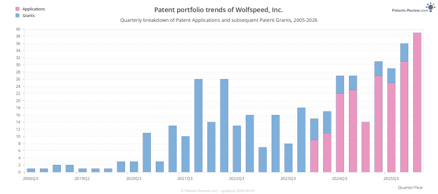
Recent patent applications by Wolfspeed, Inc.
Wolfspeed, Inc. based in Durham, US has been assigned the rights to these inventions. The list includes both Pending Applications and Patent Grants:
US20250379058A1
ElectricitySurface Processing of Semiconductor Workpieces
#2 | 2025-11-11 ✅ Patent 12,469,682 granted on 2025-11-11US18662033
ElectricityElectrical discharge machining processing for semiconductor workpiece
#3 | 2025-10-28 ✅ Patent 12,454,768 granted on 2025-10-28US18941479
Chemistry; metallurgyHybrid seed structure for crystal growth system
#4 | 2025-10-07 ✅ Patent 12,438,001 granted on 2025-10-07US18628246
ElectricityOff axis laser-based surface processing operations for semiconductor wafers
#5 | 2025-10-07 ✅ Patent 12,434,330 granted on 2025-10-07US18628223
Performing operations; transportingLaser-based surface processing for semiconductor workpiece
#6 | 2025-09-11 ✅ Patent 12,610,767 granted on 2026-04-21US20250285873A1
ElectricityAdditives for Grinding Semiconductor Workpieces
#7 | 2025-09-11 ✅ Patent 12,521,840 granted on 2026-01-13US20250282022A1
Performing operations; transportingTwo Component Chemical Mechanical Polishing
#8 | 2025-09-11 ✅ Patent 12,533,767 granted on 2026-01-27US20250282016A1
Performing operations; transportingGrind Wheel Design for Low Edge-Roll Grinding
#9 | 2025-07-15 ✅ Patent 12,362,237 granted on 2025-07-15US18628231
ElectricityFill-in planarization system and method
#10 | 2025-06-26 ✅ Patent 12,512,658 granted on 2025-12-30US20250210962A1
ElectricityDEVICE HAVING A RATE OF CURRENT CHANGE LIMITER AND PROCESS OF IMPLEMENTING THE SAME
#11 | 2025-06-03 ✅ Patent 12,322,087 granted on 2025-06-03US18674427
PhysicsMulti-scale autoencoders for semiconductor workpiece understanding
#12 | 2025-05-27 ✅ Patent 12,315,729 granted on 2025-05-27US18661994
ElectricityLaser-based processing for semiconductor wafers
#13 | 2025-04-08 ✅ Patent 12,269,123 granted on 2025-04-08US18628275
Performing operations; transportingLaser edge shaping for semiconductor wafers
#14 | 2024-12-12 ✅ Patent 12,392,821 granted on 2025-08-19US20240410939A1
PhysicsImproved Thermal and Electrical Conductivity Between Metal Contacts
#15 | 2024-10-24 ✅ Patent 12,473,661 granted on 2025-11-18US20240352622A1
Chemistry; metallurgyLARGE DIAMETER SILICON CARBIDE WAFERS
#16 | 2024-10-10 ✅ Patent 12,402,240 granted on 2025-08-26US20240341026A1
ElectricitySILICON CARBIDE THERMAL BRIDGE INTEGRATED ON A LOW THERMAL CONDUCTIVITY SUBSTRATE AND PROCESSES IMPLEMENTING THE SAME
#17 | 2024-10-03 ✅ Patent 12,402,380 granted on 2025-08-26US20240332352A1
ElectricityNONDESTRUCTIVE CHARACTERIZATION FOR CRYSTALLINE WAFERS
#18 | 2024-09-12 ✅ Patent 12,563,760 granted on 2026-02-24US20240304702A1
ElectricityField Reducing Structures for Nitrogen-Polar Group III-Nitride Semiconductor Devices
#19 | 2024-08-29 ✅ Patent 12,446,180 granted on 2025-10-14US20240292575A1
ElectricityHigh Power Multilayer Module Having Low Inductance and Fast Switching for Paralleling Power Devices
#20 | 2024-08-22 ✅ Patent 12,588,521 granted on 2026-03-24US20240282741A1
ElectricityMetal Nitride Core-Shell Particle Die-Attach Material
#21 | 2024-08-15 ✅ Patent 12,199,071 granted on 2025-01-14US20240274584A1
ElectricityCompact power module
#22 | 2024-07-04 ✅ Patent 12,500,585 granted on 2025-12-16US20240223176A1
ElectricityOPTIMIZATION OF POWER MODULE PERFORMANCE VIA PARASITIC MUTUAL COUPLING
#23 | 2024-06-27 ✅ Patent 12,593,697 granted on 2026-03-31US20240213184A1
ElectricityINTEGRATED PASSIVE DEVICES (IPD) HAVING A BASEBAND DAMPING RESISTOR FOR RADIOFREQUENCY POWER DEVICES AND DEVICES AND PROCESSES IMPLEMENTING THE SAME
#24 | 2024-06-13 ✅ Patent 12,535,518 granted on 2026-01-27US20240192261A1
PhysicsMULTIPLE TRANSPORT LEVEL TESTER SYSTEM
#25 | 2024-06-13 ✅ Patent 12,594,622 granted on 2026-04-07US20240189940A1
Performing operations; transportingLASER-ASSISTED METHOD FOR PARTING CRYSTALLINE MATERIAL
#26 | 2024-05-30 ✅ Patent 12,289,906 granted on 2025-04-29US20240178314A1
ElectricityVertical power devices fabricated using implanted methods
#27 | 2024-03-28 ✅ Patent 12,477,770 granted on 2025-11-18US20240105829A1
ElectricityGROUP III-NITRIDE HIGH-ELECTRON MOBILITY TRANSISTORS WITH BURIED P-TYPE LAYERS AND PROCESS FOR MAKING THE SAME
#28 | 2024-03-28 ✅ Patent 12,400,986 granted on 2025-08-26US20240105651A1
ElectricityPACKAGE FOR POWER ELECTRONICS
#29 | 2024-03-28 ✅ Patent 12,620,530 granted on 2026-05-05US20240105390A1
ElectricityDEVICE AND PROCESS FOR IMPLEMENTING SILICON CARBIDE (SIC) SURFACE MOUNT DEVICES
#30 | 2024-02-29 ✅ Patent 12,159,909 granted on 2024-12-03US20240072131A1
ElectricityPower semiconductor device with reduced strain
#31 | 2023-12-28 ✅ Patent 11,936,368 granted on 2024-03-19US20230421145A1
ElectricityOptimization of power module performance via parasitic mutual coupling
#32 | 2023-12-28 ✅ Patent 12,470,185 granted on 2025-11-11US20230421119A1
ElectricitySEMICONDUCTOR DEVICE PACKAGES WITH EXPOSED HEAT DISSIPATING SURFACES AND METHODS OF FABRICATING THE SAME
#33 | 2023-12-28 ✅ Patent 12,550,744 granted on 2026-02-10US20230421117A1
ElectricityPACKAGES WITH BACKSIDE MOUNTED DIE AND EXPOSED DIE INTERCONNECTS AND METHODS OF FABRICATING THE SAME
#34 | 2023-12-28 ✅ Patent 12,532,488 granted on 2026-01-20US20230420577A1
ElectricitySEMICONDUCTOR DEVICE WITH SELECTIVELY GROWN FIELD OXIDE LAYER IN EDGE TERMINATION REGION
#35 | 2023-12-28 ✅ Patent 12,439,664 granted on 2025-10-07US20230420536A1
ElectricityMETHODS OF FORMING OHMIC CONTACTS ON SEMICONDUCTOR DEVICES WITH TRENCH/MESA STRUCTURES
#36 | 2023-12-28 ✅ Patent 12,641,853 granted on 2026-05-26US20230420527A1
ElectricityGATE TRENCH POWER SEMICONDUCTOR DEVICES HAVING IMPROVED BREAKDOWN PERFORMANCE AND METHODS OF FORMING SUCH DEVICES
#37 | 2023-12-28 ✅ Patent 12,446,300 granted on 2025-10-14US20230420451A1
ElectricitySEMICONDUCTOR DEVICES HAVING ON-CHIP GATE RESISTORS
#38 | 2023-12-21 ✅ Patent 12,648,187 granted on 2026-06-02US20230411446A1
ElectricityGATE TRENCH POWER SEMICONDUCTOR DEVICES HAVING TRENCH SHIELDING PATTERNS FORMED DURING THE WELL IMPLANT AND RELATED METHODS
#39 | 2023-12-21 ✅ Patent 12,374,660 granted on 2025-07-29US20230411359A1
ElectricityPOWER MODULE
#40 | 2023-12-07 ✅ Patent 12,550,350 granted on 2026-02-10US20230395695A1
ElectricityMETHOD FOR REDUCING PARASITIC CAPACITANCE AND INCREASING PEAK TRANSCONDUCTANCE WHILE MAINTAINING ON-STATE RESISTANCE AND RELATED DEVICES
#41 | 2023-11-16 ✅ Patent 12,408,360 granted on 2025-09-02US20230369445A1
ElectricityVERTICAL POWER DEVICES HAVING MESAS AND ETCHED TRENCHES THEREBETWEEN
#42 | 2023-11-09 ✅ Patent 12,150,258 granted on 2024-11-19US20230363097A1
ElectricityDual inline power module
#43 | 2023-11-09 ✅ Patent 12,315,830 granted on 2025-05-27US20230361059A1
ElectricityGroup III nitride-based monolithic microwave integrated circuits including static random access memory blocks with associated addressing and buffering circuits
#44 | 2023-11-02 ✅ Patent 12,125,806 granted on 2024-10-22US20230352425A1
ElectricityElectronic device packages with internal moisture barriers
#45 | 2023-11-02 ✅ Patent 12,438,103 granted on 2025-10-07US20230352424A1
ElectricityTRANSISTOR INCLUDING A DISCONTINUOUS BARRIER LAYER
#46 | 2023-10-19 ✅ Patent 12,080,635 granted on 2024-09-03US20230335473A1
ElectricityPower module
#47 | 2023-10-12 ✅ Patent 12,647,083 granted on 2026-06-02US20230327624A1
ElectricityRF AMPLIFIER DEVICES AND METHODS OF MANUFACTURING INCLUDING MODULARIZED DESIGNS WITH FLIP CHIP INTERCONNECTIONS AND INTEGRATION INTO PACKAGING
#48 | 2023-10-05 ✅ Patent 12,550,406 granted on 2026-02-10US20230317670A1
ElectricityPACKAGED ELECTRONIC DEVICES HAVING TRANSIENT LIQUID PHASE SOLDER JOINTS AND METHODS OF FORMING SAME
#49 | 2023-09-28 ✅ Patent 12,376,319 granted on 2025-07-29US20230307529A1
ElectricitySUPPORT SHIELD STRUCTURES FOR TRENCHED SEMICONDUCTOR DEVICES
#50 | 2023-08-24 ✅ Patent 12,426,341 granted on 2025-09-23US20230268407A1
ElectricitySEMICONDUCTOR DEVICES HAVING GATE RESISTORS WITH LOW VARIATION IN RESISTANCE VALUES
#51 | 2023-08-17 ✅ Patent 12,224,318 granted on 2025-02-11US20230261054A1
ElectricityRadio frequency transistor amplifiers having self-aligned double implanted source/drain regions for improved on-resistance performance and related methods
#52 | 2023-08-17 ✅ Patent 12,224,218 granted on 2025-02-11US20230260861A1
ElectricitySemiconductor packages with increased power handling
#53 | 2023-08-03 ✅ Patent 12,317,559 granted on 2025-05-27US20230246073A1
ElectricityWide bandgap unipolar/bipolar transistor
#54 | 2023-08-03 ✅ Patent 12,070,875 granted on 2024-08-27US20230241803A1
Performing operations; transportingSilicon carbide wafers with relaxed positive bow and related methods
#55 | 2023-07-20 ✅ Patent 12,278,284 granted on 2025-04-15US20230231047A1
ElectricityPower semiconductor devices including a trenched gate and methods of forming such devices
#56 | 2023-07-06 ✅ Patent 12,315,836 granted on 2025-05-27US20230215833A1
ElectricityLimiting failures caused by dendrite growth on semiconductor chips
#57 | 2023-06-29 ✅ Patent 11,837,657 granted on 2023-12-05US20230207686A1
ElectricityGate trench power semiconductor devices having improved deep shield connection patterns
#58 | 2023-06-22 ✅ Patent 12,324,179 granted on 2025-06-03US20230197841A1
ElectricityGroup III-nitride high-electron mobility transistors with a buried metallic conductive material layer and process for making the same
#59 | 2023-06-08 ✅ Patent 12,376,332 granted on 2025-07-29US20230178650A1
ElectricityEDGE TERMINATION STRUCTURES FOR SEMICONDUCTOR DEVICES
#60 | 2023-06-01 ✅ Patent 12,009,389 granted on 2024-06-11US20230170383A1
ElectricityEdge termination for power semiconductor devices and related fabrication methods
#61 | 2023-06-01 ✅ Patent 12,438,097 granted on 2025-10-07US20230170306A1
ElectricityINTEGRATED POWER MODULE
#62 | 2023-05-25 ✅ Patent 12,087,680 granted on 2024-09-10US20230163062A1
ElectricityPower module having an elevated power plane with an integrated signal board and process of implementing the same
#63 | 2023-05-25 ✅ Patent 12,119,239 granted on 2024-10-15US20230162991A1
ElectricityPackaged semiconductor devices, and package molds for forming packaged semiconductor devices
#64 | 2023-05-18 ✅ Patent 12,393,214 granted on 2025-08-19US20230152830A1
PhysicsDEVICE DESIGN FOR SHORT-CIRCUIT PROTECTION OF TRANSISTORS
#65 | 2023-05-11 ✅ Patent 11,923,344 granted on 2024-03-05US20230142930A1
ElectricityCompact power module
#66 | 2023-04-27 ✅ Patent 12,113,114 granted on 2024-10-08US20230130614A1
ElectricityTransistor with ohmic contacts
#67 | 2023-04-20 ✅ Patent 12,300,564 granted on 2025-05-13US20230124581A1
ElectricityTransistor device structure with angled wire bonds
#68 | 2023-04-20 ✅ Patent 12,653,026 granted on 2026-06-09US20230120729A1
ElectricityPOWER SEMICONDUCTOR DEVICES INCLUDING MULTIPLE GATE BOND PADS
#69 | 2023-03-23 ✅ Patent 11,894,455 granted on 2024-02-06US20230087937A1
ElectricityVertical power devices fabricated using implanted methods
#70 | 2023-03-16 ✅ Patent 12,218,202 granted on 2025-02-04US20230078017A1
ElectricitySemiconductor device incorporating a substrate recess
#71 | 2023-03-02 ✅ Patent 11,984,433 granted on 2024-05-14US20230060641A1
ElectricityArrangements of power semiconductor devices for improved thermal performance
#72 | 2023-02-09 ✅ Patent 12,289,057 granted on 2025-04-29US20230040992A1
ElectricityCircuits and methods for controlling bidirectional CLLC converters
#73 | 2023-02-09 ✅ Patent 11,621,672 granted on 2023-04-04US20230040260A1
ElectricityCompensation of trapping in field effect transistors
#74 | 2023-02-02 ✅ Patent 11,842,937 granted on 2023-12-12US20230031205A1
ElectricityEncapsulation stack for improved humidity performance and related fabrication methods
#75 | 2023-01-26 ✅ Patent 11,810,912 granted on 2023-11-07US20230026868A1
ElectricitySemiconductor devices having asymmetric integrated gate resistors for balanced turn-on/turn-off behavior
#76 | 2022-12-29 ✅ Patent 12,087,854 granted on 2024-09-10US20220416075A1
ElectricityVertical semiconductor device with improved ruggedness
#77 | 2022-12-22 ✅ Patent 12,024,794 granted on 2024-07-02US20220403552A1
Chemistry; metallurgyReduced optical absorption for silicon carbide crystalline materials
#78 | 2022-12-15 ✅ Patent 11,935,879 granted on 2024-03-19US20220399318A1
ElectricityIntegrated passive device (IPD) components and a package and processes implementing the same
#79 | 2022-12-08 ✅ Patent 11,843,240 granted on 2023-12-12US20220393460A1
ElectricityDevice and process for fault detection of a power device
#80 | 2022-12-01 ✅ Patent 12,598,994 granted on 2026-04-07US20220384366A1
ElectricityMULTILAYER ENCAPSULATION FOR HUMIDITY ROBUSTNESS AND RELATED FABRICATION METHODS
#81 | 2022-11-24 ✅ Patent 11,869,964 granted on 2024-01-09US20220376106A1
ElectricityField effect transistors with modified access regions
#82 | 2022-11-24 ✅ Patent 12,402,348 granted on 2025-08-26US20220376105A1
ElectricityFIELD EFFECT TRANSISTOR WITH SELECTIVE CHANNEL LAYER DOPING
#83 | 2022-11-24 ✅ Patent 12,575,125 granted on 2026-03-10US20220376098A1
ElectricityFIELD EFFECT TRANSISTOR WITH SELECTIVE MODIFIED ACCESS REGIONS
#84 | 2022-11-17 ✅ Patent 12,557,322 granted on 2026-02-17US20220367697A1
ElectricityGROUP III-NITRIDE TRANSISTORS WITH BACK BARRIER STRUCTURES AND BURIED P-TYPE LAYERS AND METHODS THEREOF
#85 | 2022-11-17 ✅ Patent 11,929,428 granted on 2024-03-12US20220367696A1
ElectricityCircuits and group III-nitride high-electron mobility transistors with buried p-type layers improving overload recovery and process for implementing the same
#86 | 2022-11-17 ✅ Patent 12,402,346 granted on 2025-08-26US20220367695A1
ElectricityCIRCUITS AND GROUP III-NITRIDE TRANSISTORS WITH BURIED P-LAYERS AND CONTROLLED GATE VOLTAGES AND METHODS THEREOF
#87 | 2022-11-03 ✅ Patent 11,696,417 granted on 2023-07-04US20220354014A1
ElectricityHigh power multilayer module having low inductance and fast switching for paralleling power devices
#88 | 2022-10-27 ✅ Patent 12,142,674 granted on 2024-11-12US20220344500A1
ElectricityGallium Nitride high-electron mobility transistors with p-type layers and process for making the same
#89 | 2022-10-13 ✅ Patent 12,322,886 granted on 2025-06-03US20220328990A1
ElectricityPower module having electrical interconnections using mechanical fittings and process of implementing the same
#90 | 2022-09-29 ✅ Patent 11,784,613 granted on 2023-10-10US20220311392A1
ElectricityHigh output power density radio frequency transistor amplifiers in flat no-lead overmold packages
#91 | 2022-09-22 ✅ Patent 12,266,721 granted on 2025-04-01US20220302291A1
ElectricityField effect transistor with multiple stepped field plate
#92 | 2022-09-22 ✅ Patent 11,757,013 granted on 2023-09-12US20220302272A1
ElectricityDrain and/or gate interconnect and finger structure
#93 | 2022-09-22 ✅ Patent 12,107,039 granted on 2024-10-01US20220302014A1
ElectricityPower component configured for improving partial discharge performance and system and process of implementing the same
#94 | 2022-09-15 ✅ Patent 12,279,448 granted on 2025-04-15US20220293787A1
ElectricityTrench bottom shielding methods and approaches for trenched semiconductor device structures
#95 | 2022-09-01 ✅ Patent 11,664,436 granted on 2023-05-30US20220278212A1
ElectricitySemiconductor devices having gate resistors with low variation in resistance values
#96 | 2022-08-18 ✅ Patent 11,869,948 granted on 2024-01-09US20220262909A1
ElectricityPower semiconductor device with reduced strain
#97 | 2022-08-18 ✅ Patent 11,569,174 granted on 2023-01-31US20220262735A1
ElectricityIntegrated power module
#98 | 2022-07-28 ✅ Patent 12,224,233 granted on 2025-02-11US20220238426A1
ElectricityPackaged electronic devices having dielectric substrates with thermally conductive adhesive layers
#99 | 2022-07-14 ✅ Patent 11,791,389 granted on 2023-10-17US20220223700A1
ElectricityRadio frequency transistor amplifiers having widened and/or asymmetric source/drain regions for improved on-resistance performance
#100 | 2022-07-14 ✅ Patent 11,908,823 granted on 2024-02-20US20220223559A1
ElectricityDevices incorporating stacked bonds and methods of forming the same
Also check out Wolfspeed, Inc.'s (Durham, United States) applicant profile with 417 patent applications submitted.
348429 ⎘