Stacked die package
US20060220262A1
2006-10-05
11/098,780
2005-04-04
✅ Patent granted
US 7,326,592 B2
2008-02-05
-
-
Steven Loke | Earl Taylor
2025-10-22
Abstract:
A stacked die package includes a substrate or interposer board that includes a contact area on a top surface and landing pads surrounding the contact area. Solder pads are disposed on an opposite side of the substrate. The solder pads are electrically connected with the landing pads by inner board wiring. A reconstituted die, which includes a die surrounded by a frame, is mounted over the substrate. A top die is mounted over the reconstituted die. Both the reconstituted die and the top die are electrically connected to the substrate, e.g., by wire bonds.
Assignee:
- Infineon Technologies AG 4,173 🇩🇪 Munich, Germany
Interested in similar patents?
Get notified when new applications in this technology area are published.
Classification:
H01L21/6835 » CPC main
Processes or apparatus adapted for the manufacture or treatment of semiconductor or solid state devices or of parts thereof; Apparatus specially adapted for handling semiconductor or electric solid state devices during manufacture or treatment thereof; Apparatus specially adapted for handling wafers during manufacture or treatment of semiconductor or electric solid state devices or components ; Apparatus not specifically provided for elsewhere for supporting or gripping using temporarily an auxiliary support
H01L21/568 » CPC further
Processes or apparatus adapted for the manufacture or treatment of semiconductor or solid state devices or of parts thereof; Manufacture or treatment of semiconductor devices or of parts thereof the devices having at least one potential-jump barrier or surface barrier, e.g. PN junction, depletion layer or carrier concentration layer; Assembly of semiconductor devices using processes or apparatus not provided for in a single one of the subgroups - , e.g. sealing of a cap to a base of a container; Encapsulations, e.g. encapsulation layers, coatings Temporary substrate used as encapsulation process aid
H01L23/3128 » CPC further
Details of semiconductor or other solid state devices; Encapsulations, e.g. encapsulating layers, coatings, e.g. for protection characterised by the arrangement or shape the device being completely enclosed a substrate forming part of the encapsulation the substrate having spherical bumps for external connection
H01L24/33 » CPC further
Arrangements for connecting or disconnecting semiconductor or solid-state bodies; Methods or apparatus related thereto; Means for bonding being attached to, or being formed on, the surface to be connected, e.g. chip-to-package, die-attach, "first-level" interconnects; Manufacturing methods related thereto; Layer connectors, e.g. plate connectors, solder or adhesive layers; Manufacturing methods related thereto; Structure, shape, material or disposition of the layer connectors after the connecting process of a plurality of layer connectors
H01L24/49 » CPC further
Arrangements for connecting or disconnecting semiconductor or solid-state bodies; Methods or apparatus related thereto; Means for bonding being attached to, or being formed on, the surface to be connected, e.g. chip-to-package, die-attach, "first-level" interconnects; Manufacturing methods related thereto; Wire connectors; Manufacturing methods related thereto; Structure, shape, material or disposition of the wire connectors after the connecting process of a plurality of wire connectors
H01L24/83 » CPC further
Arrangements for connecting or disconnecting semiconductor or solid-state bodies; Methods or apparatus related thereto; Methods for connecting semiconductor or other solid state bodies using means for bonding being attached to, or being formed on, the surface to be connected using a layer connector
H01L24/85 » CPC further
Arrangements for connecting or disconnecting semiconductor or solid-state bodies; Methods or apparatus related thereto; Methods for connecting semiconductor or other solid state bodies using means for bonding being attached to, or being formed on, the surface to be connected using a wire connector
H01L24/96 » CPC further
Arrangements for connecting or disconnecting semiconductor or solid-state bodies; Methods or apparatus related thereto; Batch processes at chip-level, i.e. with connecting carried out on a plurality of singulated devices, i.e. on diced chips the devices being encapsulated in a common layer, e.g. neo-wafer or pseudo-wafer, said common layer being separable into individual assemblies after connecting
H01L24/97 » CPC further
Arrangements for connecting or disconnecting semiconductor or solid-state bodies; Methods or apparatus related thereto; Batch processes at chip-level, i.e. with connecting carried out on a plurality of singulated devices, i.e. on diced chips the devices being connected to a common substrate, e.g. interposer, said common substrate being separable into individual assemblies after connecting
H01L25/50 » CPC further
Assemblies consisting of a plurality of individual semiconductor or other solid state devices ; Multistep manufacturing processes thereof Multistep manufacturing processes of assemblies consisting of devices, each device being of a type provided for in group or
H01L24/48 » CPC further
Arrangements for connecting or disconnecting semiconductor or solid-state bodies; Methods or apparatus related thereto; Means for bonding being attached to, or being formed on, the surface to be connected, e.g. chip-to-package, die-attach, "first-level" interconnects; Manufacturing methods related thereto; Wire connectors; Manufacturing methods related thereto; Structure, shape, material or disposition of the wire connectors after the connecting process of an individual wire connector
H01L24/73 » CPC further
Arrangements for connecting or disconnecting semiconductor or solid-state bodies; Methods or apparatus related thereto Means for bonding being of different types provided for in two or more of groups , , , , , , ,
H01L2224/0401 » CPC further
Indexing scheme for arrangements for connecting or disconnecting semiconductor or solid-state bodies and methods related thereto as covered by; Means for bonding being attached to, or being formed on, the surface to be connected, e.g. chip-to-package, die-attach, "first-level" interconnects; Manufacturing methods related thereto; Bonding areas; Manufacturing methods related thereto; Structure, shape, material or disposition of the bonding areas prior to the connecting process Bonding areas specifically adapted for bump connectors, e.g. under bump metallisation [UBM]
H01L2224/04105 » CPC further
Indexing scheme for arrangements for connecting or disconnecting semiconductor or solid-state bodies and methods related thereto as covered by; Means for bonding being attached to, or being formed on, the surface to be connected, e.g. chip-to-package, die-attach, "first-level" interconnects; Manufacturing methods related thereto; Bonding areas; Manufacturing methods related thereto; Structure, shape, material or disposition of the bonding areas prior to the connecting process Bonding areas formed on an encapsulation of the semiconductor or solid-state body, e.g. bonding areas on chip-scale packages
H01L2224/20 » CPC further
Indexing scheme for arrangements for connecting or disconnecting semiconductor or solid-state bodies and methods related thereto as covered by; Means for bonding being attached to, or being formed on, the surface to be connected, e.g. chip-to-package, die-attach, "first-level" interconnects; Manufacturing methods related thereto; High density interconnect [HDI] connectors; Manufacturing methods related thereto Structure, shape, material or disposition of high density interconnect preforms
H01L2224/49051 » CPC further
Indexing scheme for arrangements for connecting or disconnecting semiconductor or solid-state bodies and methods related thereto as covered by; Means for bonding being attached to, or being formed on, the surface to be connected, e.g. chip-to-package, die-attach, "first-level" interconnects; Manufacturing methods related thereto; Wire connectors; Manufacturing methods related thereto; Structure, shape, material or disposition of the wire connectors after the connecting process of a plurality of wire connectors; Shape Connectors having different shapes
H01L2224/8385 » CPC further
Indexing scheme for arrangements for connecting or disconnecting semiconductor or solid-state bodies and methods related thereto as covered by; Methods for connecting semiconductor or other solid state bodies using means for bonding being attached to, or being formed on, the surface to be connected using a layer connector; Bonding techniques using a polymer adhesive, e.g. an adhesive based on silicone, epoxy, polyimide, polyester
H01L2224/85001 » CPC further
Indexing scheme for arrangements for connecting or disconnecting semiconductor or solid-state bodies and methods related thereto as covered by; Methods for connecting semiconductor or other solid state bodies using means for bonding being attached to, or being formed on, the surface to be connected using a wire connector involving a temporary auxiliary member not forming part of the bonding apparatus, e.g. removable or sacrificial coating, film or substrate
H01L2225/0651 » CPC further
Details relating to assemblies covered by the group but not provided for in its subgroups; All the devices being of a type provided for in the same subgroup of groups - the devices not having separate containers the devices being of a type provided for in group; Stacked arrangements of devices Wire or wire-like electrical connections from device to substrate
H01L2225/06527 » CPC further
Details relating to assemblies covered by the group but not provided for in its subgroups; All the devices being of a type provided for in the same subgroup of groups - the devices not having separate containers the devices being of a type provided for in group; Stacked arrangements of devices Special adaptation of electrical connections, e.g. rewiring, engineering changes, pressure contacts, layout
H01L2225/06555 » CPC further
Details relating to assemblies covered by the group but not provided for in its subgroups; All the devices being of a type provided for in the same subgroup of groups - the devices not having separate containers the devices being of a type provided for in group; Stacked arrangements of devices Geometry of the stack, e.g. form of the devices, geometry to facilitate stacking
H01L2225/06593 » CPC further
Details relating to assemblies covered by the group but not provided for in its subgroups; All the devices being of a type provided for in the same subgroup of groups - the devices not having separate containers the devices being of a type provided for in group; Stacked arrangements of devices Mounting aids permanently on device; arrangements for alignment
H01L2924/01004 » CPC further
Indexing scheme for arrangements or methods for connecting or disconnecting semiconductor or solid-state bodies as covered by; Chemical elements Beryllium [Be]
H01L2924/01005 » CPC further
Indexing scheme for arrangements or methods for connecting or disconnecting semiconductor or solid-state bodies as covered by; Chemical elements Boron [B]
H01L2924/01006 » CPC further
Indexing scheme for arrangements or methods for connecting or disconnecting semiconductor or solid-state bodies as covered by; Chemical elements Carbon [C]
H01L2924/01014 » CPC further
Indexing scheme for arrangements or methods for connecting or disconnecting semiconductor or solid-state bodies as covered by; Chemical elements Silicon [Si]
H01L2924/01028 » CPC further
Indexing scheme for arrangements or methods for connecting or disconnecting semiconductor or solid-state bodies as covered by; Chemical elements Nickel [Ni]
H01L2924/01029 » CPC further
Indexing scheme for arrangements or methods for connecting or disconnecting semiconductor or solid-state bodies as covered by; Chemical elements Copper [Cu]
H01L2924/01033 » CPC further
Indexing scheme for arrangements or methods for connecting or disconnecting semiconductor or solid-state bodies as covered by; Chemical elements Arsenic [As]
H01L2924/01078 » CPC further
Indexing scheme for arrangements or methods for connecting or disconnecting semiconductor or solid-state bodies as covered by; Chemical elements Platinum [Pt]
H01L2924/01079 » CPC further
Indexing scheme for arrangements or methods for connecting or disconnecting semiconductor or solid-state bodies as covered by; Chemical elements Gold [Au]
H01L2924/014 » CPC further
Indexing scheme for arrangements or methods for connecting or disconnecting semiconductor or solid-state bodies as covered by; Alloys Solder alloys
H01L2924/07802 » CPC further
Indexing scheme for arrangements or methods for connecting or disconnecting semiconductor or solid-state bodies as covered by; Polymers; Adhesive characteristics other than chemical not being an ohmic electrical conductor
H01L2924/14 » CPC further
Indexing scheme for arrangements or methods for connecting or disconnecting semiconductor or solid-state bodies as covered by; Details of semiconductor or other solid state devices to be connected; Device type Integrated circuits
H01L2924/19107 » CPC further
Indexing scheme for arrangements or methods for connecting or disconnecting semiconductor or solid-state bodies as covered by; Details of hybrid assemblies other than the semiconductor or other solid state devices to be connected; Disposition of discrete passive components off-chip wires
H01L2224/97 » CPC further
Indexing scheme for arrangements for connecting or disconnecting semiconductor or solid-state bodies and methods related thereto as covered by; Batch processes at chip-level, i.e. with connecting carried out on a plurality of singulated devices, i.e. on diced chips the devices being connected to a common substrate, e.g. interposer, said common substrate being separable into individual assemblies after connecting
H01L2224/73265 » CPC further
Indexing scheme for arrangements for connecting or disconnecting semiconductor or solid-state bodies and methods related thereto as covered by; Means for bonding being of different types provided for in two or more of groups; Location after the connecting process on different surfaces Layer and wire connectors
H01L2224/82 » CPC further
Indexing scheme for arrangements for connecting or disconnecting semiconductor or solid-state bodies and methods related thereto as covered by; Methods for connecting semiconductor or other solid state bodies using means for bonding being attached to, or being formed on, the surface to be connected by forming build-up interconnects at chip-level, e.g. for high density interconnects [HDI]
H01L2924/00 » CPC further
Indexing scheme for arrangements or methods for connecting or disconnecting semiconductor or solid-state bodies as covered by
H01L2224/023 » CPC further
Indexing scheme for arrangements for connecting or disconnecting semiconductor or solid-state bodies and methods related thereto as covered by; Means for bonding being attached to, or being formed on, the surface to be connected, e.g. chip-to-package, die-attach, "first-level" interconnects; Manufacturing methods related thereto; Bonding areas; Manufacturing methods related thereto Redistribution layers [RDL] for bonding areas
H01L2924/0001 » CPC further
Indexing scheme for arrangements or methods for connecting or disconnecting semiconductor or solid-state bodies as covered by Technical content checked by a classifier
H01L23/48 IPC
Details of semiconductor or other solid state devices Arrangements for conducting electric current to or from the solid state body in operation, e.g. leads, terminal arrangements ; Selection of materials therefor
H01L2224/78 » CPC further
Indexing scheme for arrangements for connecting or disconnecting semiconductor or solid-state bodies and methods related thereto as covered by; Apparatus for manufacturing arrangements for connecting or disconnecting semiconductor or solid-state bodies and for methods related thereto Apparatus for connecting with wire connectors
H01L2224/83192 » CPC further
Indexing scheme for arrangements for connecting or disconnecting semiconductor or solid-state bodies and methods related thereto as covered by; Methods for connecting semiconductor or other solid state bodies using means for bonding being attached to, or being formed on, the surface to be connected using a layer connector; Arrangement of the layer connectors prior to mounting wherein the layer connectors are disposed only on another item or body to be connected to the semiconductor or solid-state body
H01L2224/4903 » CPC further
Indexing scheme for arrangements for connecting or disconnecting semiconductor or solid-state bodies and methods related thereto as covered by; Means for bonding being attached to, or being formed on, the surface to be connected, e.g. chip-to-package, die-attach, "first-level" interconnects; Manufacturing methods related thereto; Wire connectors; Manufacturing methods related thereto; Structure, shape, material or disposition of the wire connectors after the connecting process of a plurality of wire connectors; Structure Connectors having different sizes, e.g. different diameters
H01L2924/15311 » CPC further
Indexing scheme for arrangements or methods for connecting or disconnecting semiconductor or solid-state bodies as covered by; Details of package parts other than the semiconductor or other solid state devices to be connected; Die mounting substrate; Connection portion the connection portion being formed only on the surface of the substrate opposite to the die mounting surface being a ball array, e.g. BGA
H01L2924/10253 » CPC further
Indexing scheme for arrangements or methods for connecting or disconnecting semiconductor or solid-state bodies as covered by; Details of semiconductor or other solid state devices to be connected; Material of the semiconductor or solid state bodies; Semiconducting materials; Elemental semiconductors, i.e. Group IV Silicon [Si]
H01L2924/15747 » CPC further
Indexing scheme for arrangements or methods for connecting or disconnecting semiconductor or solid-state bodies as covered by; Details of package parts other than the semiconductor or other solid state devices to be connected; Die mounting substrate; Material with a principal constituent of the material being a metal or a metalloid, e.g. boron [B], silicon [Si], germanium [Ge], arsenic [As], antimony [Sb], tellurium [Te] and polonium [Po], and alloys thereof the principal constituent melting at a temperature of greater than or equal to 950 C and less than 1550 C Copper [Cu] as principal constituent
H01L2224/45099 » CPC further
Indexing scheme for arrangements for connecting or disconnecting semiconductor or solid-state bodies and methods related thereto as covered by; Means for bonding being attached to, or being formed on, the surface to be connected, e.g. chip-to-package, die-attach, "first-level" interconnects; Manufacturing methods related thereto; Wire connectors; Manufacturing methods related thereto; Structure, shape, material or disposition of the wire connectors prior to the connecting process of an individual wire connector; Core members of the connector Material
H01L2924/00014 » CPC further
Indexing scheme for arrangements or methods for connecting or disconnecting semiconductor or solid-state bodies as covered by; Technical content checked by a classifier the subject-matter covered by the group, the symbol of which is combined with the symbol of this group, being disclosed without further technical details
H01L2224/05599 » CPC further
Indexing scheme for arrangements for connecting or disconnecting semiconductor or solid-state bodies and methods related thereto as covered by; Means for bonding being attached to, or being formed on, the surface to be connected, e.g. chip-to-package, die-attach, "first-level" interconnects; Manufacturing methods related thereto; Bonding areas; Manufacturing methods related thereto; Structure, shape, material or disposition of the bonding areas prior to the connecting process of an individual bonding area; External layer Material
H01L2924/181 » CPC further
Indexing scheme for arrangements or methods for connecting or disconnecting semiconductor or solid-state bodies as covered by; Details of package parts other than the semiconductor or other solid state devices to be connected Encapsulation
H01L2924/00012 » CPC further
Indexing scheme for arrangements or methods for connecting or disconnecting semiconductor or solid-state bodies as covered by; Technical content checked by a classifier Relevant to the scope of the group, the symbol of which is combined with the symbol of this group
H01L21/782 IPC
Processes or apparatus adapted for the manufacture or treatment of semiconductor or solid state devices or of parts thereof; Manufacture or treatment of devices consisting of a plurality of solid state components formed in or on a common substrate or of parts thereof; Manufacture of integrated circuit devices or of parts thereof; Manufacture or treatment of devices consisting of a plurality of solid state components or integrated circuits formed in, or on, a common substrate with subsequent division of the substrate into plural individual devices to produce devices, each consisting of a single circuit element
Description
TECHNICAL FIELDThe invention relates to a stacked die package with integrated circuits such as memory devices or controllers.
BACKGROUNDThe development of the application of integrated circuits shows that more complex functions are to be realized but there are limitations of the number of functions realizable on a single chip. Therefore, technologies for stacking of two or more dies with several functions and methods for the mechanical and electrical interconnection with one another or with a base substrate which is the basis for stacking and for mounting on a PCB (Printed Circuit Board) have been developed.
Several technologies for contacting different chips are known. Conventional technologies are using chip and wire bonding for contacting the dies electrically. These are known processes with well-known parameters. Using these technologies for stacked dies (FBGA: fine ball grid array) the chips are placed one over another and the contacts of the dies are connected with corresponding contact pads on the substrate by wire loops performed by bonding.
For this wire bonding it is necessary to reroute the bond pads, which are typically arranged in a row at the die center, to the edge of the die, to avoid long wire bond loops (electrical performance). The rerouting (redistribution layer, RDL) is typically a metal line made of copper (basis metal), nickel (covering layer) and gold (suitable for contacts). It can be built by electro- or electroless plating.
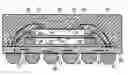
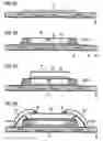
According to FIG. 1 (prior art), a first die 1 is bonded to the substrate or interposer board 2 by chip bonding. This can be performed by positioning an adhesive 3 between the first die 1 and the substrate 2. Such adhesive 3 can be a tape with an adhesive coating on both sides. Then the bond pads 4 of the first die 1 are connected with contact pads 5 on the substrate with wire loops 6 by wire bonding.
Now a distance element or spacer 7 must be mounted on the top side of the first die 1. This is possible with known technologies like die bonding with adhesive 8 or a tape. The spacer 7 is necessary for protecting the wire loop 6 between the bond pad 4 on the first die 1 and the contact pad 5 on the substrate 2. The spacer 7 can be a silicon die, an adhesive tape with a sufficient thickness or any other suitable material, but the dimensions of the spacer 7 must be smaller than the dimensions of the die 1.
After this step, a next die 9 can be mounted on the spacer 7 with adhesive 10 or tape and then the same connecting procedure must be performed like for the first die 1 including connecting the bond pads 11 on the second die 9 with contact pads 5 on the substrate 2 by wire loops 12. The stacked structure is now protected (backside- and edge protect) by a mold encapsulant 13. The substrate 2, opposite the stacked dies 1, 9 is provided with solder balls 14 which are electrically connected (normally soldered) to the contact pads 5 on the substrate 2.
It seems to be clear that this is a very expensive technology (serial processes with high accuracy), even in case that more than two dies are stacked.
The high number of interfaces (due to the spacer) results in a lower processing yield. Additionally, the top die has to be bonded on overhang, which is a critical process for very thin dies. These are needed because the absolute height of the package is increased by the spacer, but the height restrictions of stacked packages nevertheless have to be fulfilled. Furthermore, the reliability (e.g., moisture resistance) is a critical aspect due to the high number of interfaces if a spacer is used in a wire-bonded stacked package.
An example for a package of semiconductor chips is known from U.S. Patent Application Publication 2003/0015803 A1. The semiconductor chips have identical dimensions and are spaced apart by spacers of smaller lateral dimensions, preventing the chip from directly contacting to the neighbor and allowing wire-bonding of each of the stacked chips to the bonding pads on a carrier.
Another stacked multi-chip module and a method for manufacturing a stacked multi-chip module is described in EP 0 575051 B1. According to this document, a first element (die) is mounted on a substrate by using an adhesive material. A second element (die) is mounted to the first again by using an adhesive material. The third die should be at least partially supported by the second die and the second die should be at least partially supported by the first die. Furthermore, the second die is positioned such that the electrical contacts are exposed and accessible for making fine wire connections thereto. Likewise, the third die may be positioned such that electrical contacts of the second die are exposed and accessible for making fine wire connections thereto. Although the upper dies are progressively smaller in size.
The problem of this prior art is that the dies must be equal in size but it is possible to stack very thin dies.
SUMMARY OF THE INVENTIONIn one aspect, the present invention overcomes the limitations of the prior art and simplifies the assembly technology.
In another aspect, the invention increases the reliability of a stacked die package by decreasing the number of interfaces within the package.
In a further aspect, the invention decreases the total height of the package or increases the number of chips in the package with maintaining the total package height.
According to an embodiment of the invention, the bottom die can be modified in advance to die bonding to provide additional area around the silicon edge. That way the use of a spacer is not needed. The bottom die is embedded in a polymer material by molding (reconstitution) resulting in a frame around the die. This frame is a fan-out area, the chip area is now larger than the bare silicon of the die. The redistribution line that is used to distribute connections from the pads on the chip to the edges of the die package can be elongated to the edge of the frame. The position for the bond wire interconnect is transferred to the edge of the frame as well. That way the bottom die on the substrate is provided with a larger area than a next die, which can be die bonded with an adhesive at the top side of the first reconstituted die. The area out of the die shadow of the upper die can now used to connect the first die with the substrate or the bottom die by wire bonding.
The result is that a spacer is no longer necessary, all process steps, necessary for assembling the spacer can be left out. This leads to lower packaging costs and less reliability issues due to a reduced number of material interfaces.
Another feature of the invention is that more dies can be stacked at a given total height, or the total package height of two stacked dies can be reduced.
One feature of the preferred embodiment of the invention is a reconstituted die, surrounded by a polymer. A surrounding rim is performed, protecting the backside and the edge of the silicon die, and not covering the active side of the die. It is possible to provide bond pads outside the silicon area (fan-out) on the RDL.
The reconstituted chip is produced in the well-known wafer-level technology. Front-end tested good dies after dicing are picked up and placed face down on an adhesive tape with any distance from each other (fan-out area). Then, the dies on the tape are reconstituted to a reconstituted wafer-by-wafer molding with the mentioned polymer.
An RDL is formed (e.g., sputter and plate) from the center row bond pads to the edge of the reconstituted die on the wafer. At the edge of the polymer embedded die, this RDL is used as new bond pad for the wire bond to the substrate.
After applying the RDL, the reconstituted wafer is diced into individual reconstituted dies, each provided with a polymer frame. With this rerouting of the bond pads, it is possible to stack dies with a minor basic (fan-out) area (as the bottom reconstituted die) or standard front-end dies on the reconstituted bottom die. Therefore, only an adhesive without any spacer is needed.
It is also possible to stack dies with originally equal dimensions due to the provided frame, which is increasing the dimension of the bottom die.
BRIEF DESCRIPTION OF THE DRAWINGSFor a more complete understanding of the present invention, and the advantages thereof, reference is now made to the following descriptions taken in conjunction with the accompanying drawing, in which:
FIG. 1 illustrates stacked dies on an interposer board according to the prior art;
FIG. 2 illustrates an embodiment of stacked dies according to a preferred embodiment of the invention with a reconstituted die on an interposer board and a second die mounted on the reconstituted die;
FIGS. 3a to 3h show the manufacturing steps to realize reconstituted dies;
FIGS. 4a to 4f illustrate the process flow for stacking dies according to a preferred embodiment of the invention; and
FIG. 5 illustrates an example with three dies stacked on a substrate and each of the stacked dies electrically connected with the interposer board.
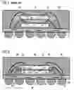
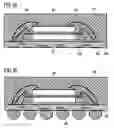
DETAILED DESCRIPTION OF ILLUSTRATIVE EMBODIMENTSFIG. 2 illustrates an embodiment of the invention with an interposer board 20 with a reconstituted die 21 mounted on the interposer board 20. The reconstituted die 21 is mounted on the interposer board 20 by a liquid adhesive 22 or an adhesive tape 22. The reconstituted die 21 is provided with a frame 23 to increase the die area (fan-out) to the mentioned reconstituted die 21. The top or active surface of the reconstituted die 21 is provided with RDL layer 24, which reroute the bond pads 25 arranged in a center row on the reconstituted die 21 to wire bond pads 26 positioned on the frame 23. The wire bond pads 26 can be connected with landing pads 27 on the interposer board 20 by wire loops 28. This interconnection can also take place in a later step after assembly of the top die(s).
Then a second die 29 is die bonded on the top surface of the reconstituted die 21 with an adhesive glue or tape 30. This die 29 can also be a reconstituted die with a smaller fan-out area than the bottom die for stacking three or more dies, or it is a front-end-chip without fan-out area, but with an RDL. The second die 29, and all following dies, is also provided with an RDL to reroute the bond pads 31 arranged in a centre row to wire bond pads 32 on the rim of the second die 29. These wire bond pads 32 are connected with landing pads 33 on the interposer board 20 or to the bond pads of the chip below by wire loops 34. The arrangement with the two stacked dies is surrounded by an encapsulant 35 so that the wire loops 28, 34 are protected.
The interposer board 20 is provided with solder balls 36 at the bottom side, which are connected with the landing pads 27, 33.
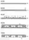
FIGS. 3a to 3h show the simplified manufacturing steps to realize reconstituted dies 21. To start, a carrier plate 40, which can be a silicon wafer or another suitable plate is provided. This plate 40 is necessary only temporarily. The plate 40 is illustrated in FIG. 3a. A releasable adhesive tape 41 is mounted on the carrier plate, as shown in FIG. 3b.
Referring to FIG. 3c, front-end tested good dies 42 are placed on the adhesive 41 with sufficient gaps between each other (fan-out area) with the active side in direction to the carrier plate. The backside and the edges of the placed dies are now molded to a reconstituted wafer, a mold encapsulant, 43 by wafer molding, as shown in FIG. 3d. In this manner, each die 42 is surrounded by a frame 44.
After this molding step the carrier plate 40 can be removed as shown in FIG. 3e. FIG. 3f illustrates the simplified step of applying the RDL 45 on the active surface of the die 42 over the interface between the chip and surrounding polymer frame 44 by sputtering, lithography and plating. The RDL can also be electroless plated or printed with any conductive material. Then a backside grinding of the die 42 is possible to remove mold compound from the backside of the dies and to decrease the thickness of the dies 42. This is shown in FIG. 3g. Referring to FIG. 3h, the reconstituted dies 21 are now separated by dicing in a way that each die 42 is surrounded by an individual frame 49.
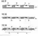
FIGS. 4a to 4f illustrate the simplified process flow for stacking of two dies according an embodiment of the invention by way of cross sections. Referring first to FIG. 4a, an interposer board 20 is provided with a die adhesive or adhesive tape 22 on its top surface at the area at which a reconstituted die 21 should be die bonded. The adhesive can be printed or the tape can be laminated in a separate step before die bonding. The interposer board is provided with landing pads 27, 33 and solder pads 46 for applying solder balls 36 (shown in FIG. 4f). The reconstituted die 21 (e.g., according FIG. 3) is die bonded to the interposer board 20.
Another adhesive layer or adhesive tape 30 is applied on the bottom die by printing, dispensing or any other technique. The next die 29 with a smaller outer dimension than the reconstituted die below 21 is die bonded now on the die below. This die 29 can be another reconstituted die or a standard front-end silicon die without fan-out area. Now the bond pads 26, 32 are connected with the landing pads 27, 33 by wire loops 28, 34, respectively. The dies can be connected as shown in FIG. 4d or the top die 29 can be connected with the die below, and this die can afterwards be connected with the interposer board 20. This bonding technique is well known and saves space in lateral dimensions. Only the chip select connection must be bonded separately between the dies.
FIG. 4e shows the stacked die assembly according to FIG. 3 after molding with a mold encapsulant 43 for mechanical protection of the silicon dies 21, 29 and wire loops 28, 34. Solder balls 36 are assembled as seen in FIG. 3f.
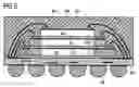
FIG. 5 shows an example with three dies 21, 29, 47 stacked on a substrate 20. The dies 21, 47 are reconstituted dies according FIG. 3h and the reconstituted die 47 has smaller dimensions than the reconstituted die 21. The frame 49 (fan-out area) of the reconstituted die 47 is smaller than the frame 23 of the reconstituted die 21. The top die 29 can be a bare die without any frame but provided with an RDL 45 or a reconstituted die as well. The lateral dimensions of the dies must shrink from bottom to top, so that wire bonding is possible from each level to the landing pads 27, 33 on the interposer board. The electrical connections are performed similar to FIG. 4d.
It is noted that the number of stacked dies is not limited.
In each of the above-described embodiments, an RDL 45 was provided to redistribute center bond pads to the peripheral of the chip. It is understood, however, that concepts of the present invention apply to chips that include bond pads formed at the peripheral. For these chips, the RDL 45 may not be necessary or may be necessary only to redistribute peripheral pads on the die to the frame 23. As a result, the invention applies equally to embodiments that do not include an RDL.
Claims
What is claimed is:1. A stacked die package, comprising:
a substrate;
a contact area on a top surface of the substrate and landing pads surrounding the contact area;
solder pads on an opposite side of the substrate, the solder pads being electrically connected with the landing pads by inner board wiring;
a reconstituted die that includes a die surrounded by a frame, the reconstituted die mounted over the substrate; and
a top die mounted over the reconstituted die.
2. The stacked die package according to claim 1, further including an adhesive between the reconstituted die and the substrate and a second adhesive between the reconstituted die and the top die.
3. The stacked die package according to claim 1, further comprising wire loops between bond pads on the reconstituted die and the landing pads on the substrate and also between bond pads on the top die and the landing pads on the substrate.
4. The stacked die package according to claim 1, wherein the frame comprises a polymer or metal material.
5. The stacked die package according to claim 1, wherein the reconstituted die includes a redistribution layer (RDL), routing from center row bond pads on the die to wire bond pads on the frame.
6. The stacked die package according to claim 5, further comprising first wire loops between the wire bond pads on the frame of the reconstituted die and the landing pads on the substrate and second wire loops between bond pads on the top die and the landing pads on the substrate.
7. The stacked die package according to claim 6, wherein the reconstituted die, the top die and the first and second wire loops are embedded in a mold compound.
8. The stacked die package according to claim 1, wherein the substrate comprises an interposer board.
9. The stacked die package according to claim 1, further comprising a second reconstituted die that includes a second die surrounded by a second frame, the second reconstituted die being smaller than the reconstituted die but larger than the top die, the second reconstituted die mounted over the reconstituted die, the top die being mounted over the second reconstituted die.
10. A stacked die package, comprising
a substrate;
a contact area on a top surface of the substrate;
landing pads on the top surface of the substrate surrounding the contact area;
solder pads on an opposite side of the substrate, the solder pads being electrically connected with the landing pads by inner board wiring;
a first reconstituted die mounted on the contact area of the substrate board; and
further reconstituted dies mounted on top of each other on the first reconstituted die, each reconstituted die including a frame, wherein the dimensions of the frames are smaller for each reconstituted die located from the first reconstituted die to a top reconstituted die.
11. A method of manufacturing a reconstituted die, the method comprising:
providing a carrier plate with an adhesive on its surface;
placing dies on the adhesive leaving gaps between adjacent dies;
wafer molding of the placed dies with a mold encapsulant such that the gaps between the dies are filled with the encapsulant;
delaminating the carrier;
generating a redistribution layer over an active surface of each die; and
separating the dies to form reconstituted dies by dicing such that each die is surrounded by an individual frame.
12. The method of claim 11, further comprising backside grinding of the dies prior to separating the dies.
13. The method of claim 11, wherein placing dies comprises placing front-end tested good dies.
14. The method of claim 11, wherein a backside of each die is overmolded during the wafer molding.
15. The method of claim 11, wherein the gaps between adjacent ones of the dies comprise gaps of varying sizes.
16. The method of claim 11, further comprising:
mounting one of the reconstituted dies over a substrate;
mounting a bare die over the one reconstituted die; and
electrically connecting the reconstituted die to the substrate.
17. The method of claim 16, further comprising electrically connecting the bare die to the substrate.
18. The method of claim 16, wherein electrically connecting the reconstituted die to the substrate comprises wirebonding from bonding pads on the reconstituted die to landing pads on the substrate.
19. The method of claim 18, wherein the bonding pads are disposed over a frame portion of the reconstituted die, the frame portion comprising the encapsulant.
20. The method of claim 11, wherein the adhesive comprises a releasable adhesive.
Images & Drawings included:
Sources:
- United States Patent and Trademark Office - verify current appl. status at the USPTO↗
Similar patent applications:
- » 20070252253
Cooling mechanism for stacked die package, and method of manufacturing stacked die package containing same - » 20120319293
MICROELECTRONIC DEVICE, STACKED DIE PACKAGE AND COMPUTING SYSTEM CONTAINING SAME, METHOD OF MANUFACTURING A MULTI-CHANNEL COMMUNICATION PATHWAY IN SAME, AND METHOD OF ENABLING ELECTRICAL COMMUNICATION BETWEEN COMPONENTS OF A STACKED-DIE PACKAGE - » 10632550
Semiconductor multi-package module including stacked-die package and having wire bond interconnect between stacked packages - » 20160099237
Microelectronic die packages with metal leads, including metal leads for stacked die packages, and associated systems and methods - » 20140015130
Microelectronic die packages with metal leads, including metal leads for stacked die packages, and associated systems and methods - » 20120241957
Microelectronic die packages with metal leads, including metal leads for stacked die packages, and associated systems and methods - » 20110068454
Microelectronic die packages with metal leads, including metal leads for stacked die packages, and associated systems and methods - » 20150091166
Microelectronic die packages with metal leads, including metal leads for stacked die packages, and associated systems and methods - » 20090026600
Microelectronic die packages with metal leads, including metal leads for stacked die packages, and associated systems and methods - » 20170207206
Microelectronic die packages with metal leads, including metal leads for stacked die packages, and associated systems and methods
Recent applications in this class:
- » 20250293073 2025-09-18
RECLAIMABLE DONOR SUBSTRATES FOR USE IN PREPARING MULTIPLE SILICON-ON-INSULATOR STRUCTURES - » 20250285904 2025-09-11
HETEROGENEOUS INTEGRATION OF COMPONENTS ONTO COMPACT DEVICES USING MOIRÉ BASED METROLOGY AND VACUUM BASED PICK-AND-PLACE - » 20250273501 2025-08-28
TEMPORARY PROTECTION FILM FOR PRODUCTION OF SEMICONDUCTOR DEVICE AND PRODUCTION METHOD FOR SEMICONDUCTOR DEVICE - » 20250259877 2025-08-14
SEMICONDUCTOR DEVICE AND MANUFACTURING METHOD OF SEMICONDUCTOR DEVICE - » 20250246475 2025-07-31
CARRIER SUBSTRATE AND METHOD OF MANUFACTURING SEMICONDUCTOR PACKAGE USING THE SAME - » 20250239477 2025-07-24
LIGHT-EMITTING ELEMENT ARRAY SUBSTRATE AND METHOD FOR MANUFACTURING LIGHT-EMITTING ELEMENT ARRAY SUBSTRATE - » 20250233002 2025-07-17
MATERIAL FOR POSITIONAL ERROR COMPENSATION IN ASSEMBLY OF DISCRETE COMPONENTS - » 20250218850 2025-07-03
SEMICONDUCTOR DEVICE ARRANGEMENT - » 20250218849 2025-07-03
WAFER BONDING APPARATUS - » 20250218848 2025-07-03
METHOD OF MANUFACTURING DISPLAY DEVICE
Recent applications for this Assignee:
- » 20190222018 2019-07-18
Temperature sensing and fault detection for paralleled double-side cooled power modules - » 20190120879 2019-04-25
Readout circuit for resistive and capacitive sensors - » 20170125556 2017-05-04
Tunnel field effect transistors - » 20160072383 2016-03-10
System and method for a controlled feedback charge pump - » 20160064451 2016-03-03
Semiconductor component comprising magnetic field sensor - » 20150137309 2015-05-21
Methods of fabricating isolation regions of semiconductor devices and structures thereof - » 20120278520 2012-11-01
System and method of transmitting data between devices connected via a bus defining a time slot during transmission for responsive output information from bus devices - » 20120199909 2012-08-09
Semiconductor devices and methods of manufacture thereof - » 20120162924 2012-06-28
Integrated Semiconductor Outline Package - » 20120081105 2012-04-05
Signal generation for spectral measurements