Microcircuit package having ductile layer
US20080128908A1
2008-06-05
11/983,813
2007-11-09
✅ Patent granted
US 7,679,185 B2
2010-03-16
-
-
Leonardo Andújar | Teresa M Arroyo
2028-02-29
Abstract:
A microcircuit package having a ductile layer between a copper flange and die attach. The ductile layer absorbs the stress between the flange and semiconductor device mounted on the flange, and can substantially reduce the stress applied to the semiconductor device. In addition, the package provides the combination of copper flange and polymeric dielectric with a TCE close to copper, which results in a low stress structure of improved reliability and conductivity.
Inventors:
- Michael A. Zimmerman 25 🇺🇸 North Andover, MA, United States
- Jonathan Harris 1 🇺🇸 Scottsdale, AZ, United States
Assignee:
- Interplex QLP, Inc. 4 🇺🇸 College Point, NY, United States
Interested in similar patents?
Get notified when new applications in this technology area are published.
Classification:
H01L2224/83805 » CPC further
Indexing scheme for arrangements for connecting or disconnecting semiconductor or solid-state bodies and methods related thereto as covered by; Methods for connecting semiconductor or other solid state bodies using means for bonding being attached to, or being formed on, the surface to be connected using a layer connector; Bonding techniques; Soldering or alloying involving forming a eutectic alloy at the bonding interface
H01L23/142 » CPC main
Details of semiconductor or other solid state devices; Mountings, e.g. non-detachable insulating substrates characterised by the material or its electrical properties Metallic substrates having insulating layers
H01L23/4924 » CPC further
Details of semiconductor or other solid state devices; Arrangements for conducting electric current to or from the solid state body in operation, e.g. leads, terminal arrangements ; Selection of materials therefor consisting of soldered constructions; Bases or plates or solder therefor characterised by the materials
H01L23/562 » CPC further
Details of semiconductor or other solid state devices Protection against mechanical damage
H01L24/29 » CPC further
Arrangements for connecting or disconnecting semiconductor or solid-state bodies; Methods or apparatus related thereto; Means for bonding being attached to, or being formed on, the surface to be connected, e.g. chip-to-package, die-attach, "first-level" interconnects; Manufacturing methods related thereto; Layer connectors, e.g. plate connectors, solder or adhesive layers; Manufacturing methods related thereto; Structure, shape, material or disposition of the layer connectors prior to the connecting process of an individual layer connector
H01L24/32 » CPC further
Arrangements for connecting or disconnecting semiconductor or solid-state bodies; Methods or apparatus related thereto; Means for bonding being attached to, or being formed on, the surface to be connected, e.g. chip-to-package, die-attach, "first-level" interconnects; Manufacturing methods related thereto; Layer connectors, e.g. plate connectors, solder or adhesive layers; Manufacturing methods related thereto; Structure, shape, material or disposition of the layer connectors after the connecting process of an individual layer connector
H01L21/4803 » CPC further
Processes or apparatus adapted for the manufacture or treatment of semiconductor or solid state devices or of parts thereof; Manufacture or treatment of semiconductor devices or of parts thereof the devices having at least one potential-jump barrier or surface barrier, e.g. PN junction, depletion layer or carrier concentration layer; Manufacture or treatment of parts, e.g. containers, prior to assembly of the devices, using processes not provided for in a single one of the subgroups - Insulating or insulated parts, e.g. mountings, containers, diamond heatsinks
H01L23/047 » CPC further
Details of semiconductor or other solid state devices; Containers; Seals characterised by the shape of the container or parts, e.g. caps, walls the container being a hollow construction and having a conductive base as a mounting as well as a lead for the semiconductor body the other leads being parallel to the base
H01L23/10 » CPC further
Details of semiconductor or other solid state devices; Containers; Seals characterised by the material or arrangement of seals between parts, e.g. between cap and base of the container or between leads and walls of the container
H01L24/48 » CPC further
Arrangements for connecting or disconnecting semiconductor or solid-state bodies; Methods or apparatus related thereto; Means for bonding being attached to, or being formed on, the surface to be connected, e.g. chip-to-package, die-attach, "first-level" interconnects; Manufacturing methods related thereto; Wire connectors; Manufacturing methods related thereto; Structure, shape, material or disposition of the wire connectors after the connecting process of an individual wire connector
H01L2924/01006 » CPC further
Indexing scheme for arrangements or methods for connecting or disconnecting semiconductor or solid-state bodies as covered by; Chemical elements Carbon [C]
H01L2924/01013 » CPC further
Indexing scheme for arrangements or methods for connecting or disconnecting semiconductor or solid-state bodies as covered by; Chemical elements Aluminum [Al]
H01L2924/01027 » CPC further
Indexing scheme for arrangements or methods for connecting or disconnecting semiconductor or solid-state bodies as covered by; Chemical elements Cobalt [Co]
H01L2924/01033 » CPC further
Indexing scheme for arrangements or methods for connecting or disconnecting semiconductor or solid-state bodies as covered by; Chemical elements Arsenic [As]
H01L2924/0104 » CPC further
Indexing scheme for arrangements or methods for connecting or disconnecting semiconductor or solid-state bodies as covered by; Chemical elements Zirconium [Zr]
H01L2924/01042 » CPC further
Indexing scheme for arrangements or methods for connecting or disconnecting semiconductor or solid-state bodies as covered by; Chemical elements Molybdenum [Mo]
H01L2924/01046 » CPC further
Indexing scheme for arrangements or methods for connecting or disconnecting semiconductor or solid-state bodies as covered by; Chemical elements Palladium [Pd]
H01L2924/01074 » CPC further
Indexing scheme for arrangements or methods for connecting or disconnecting semiconductor or solid-state bodies as covered by; Chemical elements Tungsten [W]
H01L2924/01078 » CPC further
Indexing scheme for arrangements or methods for connecting or disconnecting semiconductor or solid-state bodies as covered by; Chemical elements Platinum [Pt]
H01L2924/10329 » CPC further
Indexing scheme for arrangements or methods for connecting or disconnecting semiconductor or solid-state bodies as covered by; Details of semiconductor or other solid state devices to be connected; Material of the semiconductor or solid state bodies; Semiconducting materials; Compound semiconductors; III-V Gallium arsenide [GaAs]
H01L2924/15747 » CPC further
Indexing scheme for arrangements or methods for connecting or disconnecting semiconductor or solid-state bodies as covered by; Details of package parts other than the semiconductor or other solid state devices to be connected; Die mounting substrate; Material with a principal constituent of the material being a metal or a metalloid, e.g. boron [B], silicon [Si], germanium [Ge], arsenic [As], antimony [Sb], tellurium [Te] and polonium [Po], and alloys thereof the principal constituent melting at a temperature of greater than or equal to 950 C and less than 1550 C Copper [Cu] as principal constituent
H01L2924/16195 » CPC further
Indexing scheme for arrangements or methods for connecting or disconnecting semiconductor or solid-state bodies as covered by; Details of package parts other than the semiconductor or other solid state devices to be connected; Cap; Shape Flat cap [not enclosing an internal cavity]
H01L2924/3511 » CPC further
Indexing scheme for arrangements or methods for connecting or disconnecting semiconductor or solid-state bodies as covered by; Technical effects; Mechanical effects; Thermal stress Warping
H01L2224/73265 » CPC further
Indexing scheme for arrangements for connecting or disconnecting semiconductor or solid-state bodies and methods related thereto as covered by; Means for bonding being of different types provided for in two or more of groups; Location after the connecting process on different surfaces Layer and wire connectors
H01L2924/01082 » CPC further
Indexing scheme for arrangements or methods for connecting or disconnecting semiconductor or solid-state bodies as covered by; Chemical elements Lead [Pb]
H01L2924/01079 » CPC further
Indexing scheme for arrangements or methods for connecting or disconnecting semiconductor or solid-state bodies as covered by; Chemical elements Gold [Au]
H01L2924/3512 » CPC further
Indexing scheme for arrangements or methods for connecting or disconnecting semiconductor or solid-state bodies as covered by; Technical effects; Mechanical effects; Thermal stress Cracking
H01L2924/00 » CPC further
Indexing scheme for arrangements or methods for connecting or disconnecting semiconductor or solid-state bodies as covered by
H01L2224/45099 » CPC further
Indexing scheme for arrangements for connecting or disconnecting semiconductor or solid-state bodies and methods related thereto as covered by; Means for bonding being attached to, or being formed on, the surface to be connected, e.g. chip-to-package, die-attach, "first-level" interconnects; Manufacturing methods related thereto; Wire connectors; Manufacturing methods related thereto; Structure, shape, material or disposition of the wire connectors prior to the connecting process of an individual wire connector; Core members of the connector Material
H01L2924/00014 » CPC further
Indexing scheme for arrangements or methods for connecting or disconnecting semiconductor or solid-state bodies as covered by; Technical content checked by a classifier the subject-matter covered by the group, the symbol of which is combined with the symbol of this group, being disclosed without further technical details
H01L2924/014 » CPC further
Indexing scheme for arrangements or methods for connecting or disconnecting semiconductor or solid-state bodies as covered by; Alloys Solder alloys
H01L2924/01322 » CPC further
Indexing scheme for arrangements or methods for connecting or disconnecting semiconductor or solid-state bodies as covered by; Alloys; Binary Alloys Eutectic Alloys, i.e. obtained by a liquid transforming into two solid phases
H01L2924/207 » CPC further
Indexing scheme for arrangements or methods for connecting or disconnecting semiconductor or solid-state bodies as covered by; Parameters Diameter ranges
H01L2924/01014 » CPC further
Indexing scheme for arrangements or methods for connecting or disconnecting semiconductor or solid-state bodies as covered by; Chemical elements Silicon [Si]
H01L2924/01032 » CPC further
Indexing scheme for arrangements or methods for connecting or disconnecting semiconductor or solid-state bodies as covered by; Chemical elements Germanium [Ge]
H01L2924/0132 » CPC further
Indexing scheme for arrangements or methods for connecting or disconnecting semiconductor or solid-state bodies as covered by; Alloys Binary Alloys
H01L2924/01049 » CPC further
Indexing scheme for arrangements or methods for connecting or disconnecting semiconductor or solid-state bodies as covered by; Chemical elements Indium [In]
H01L2924/01051 » CPC further
Indexing scheme for arrangements or methods for connecting or disconnecting semiconductor or solid-state bodies as covered by; Chemical elements Antimony [Sb]
H01L2924/0103 » CPC further
Indexing scheme for arrangements or methods for connecting or disconnecting semiconductor or solid-state bodies as covered by; Chemical elements Zinc [Zn]
H01L2224/83192 » CPC further
Indexing scheme for arrangements for connecting or disconnecting semiconductor or solid-state bodies and methods related thereto as covered by; Methods for connecting semiconductor or other solid state bodies using means for bonding being attached to, or being formed on, the surface to be connected using a layer connector; Arrangement of the layer connectors prior to mounting wherein the layer connectors are disposed only on another item or body to be connected to the semiconductor or solid-state body
H01L2924/0133 » CPC further
Indexing scheme for arrangements or methods for connecting or disconnecting semiconductor or solid-state bodies as covered by; Alloys Ternary Alloys
H01L2924/01029 » CPC further
Indexing scheme for arrangements or methods for connecting or disconnecting semiconductor or solid-state bodies as covered by; Chemical elements Copper [Cu]
H01L2924/01047 » CPC further
Indexing scheme for arrangements or methods for connecting or disconnecting semiconductor or solid-state bodies as covered by; Chemical elements Silver [Ag]
H01L2924/0105 » CPC further
Indexing scheme for arrangements or methods for connecting or disconnecting semiconductor or solid-state bodies as covered by; Chemical elements Tin [Sn]
H01L23/12 IPC
Details of semiconductor or other solid state devices Mountings, e.g. non-detachable insulating substrates
H01L23/48 IPC
Details of semiconductor or other solid state devices Arrangements for conducting electric current to or from the solid state body in operation, e.g. leads, terminal arrangements ; Selection of materials therefor
H01L23/52 IPC
Details of semiconductor or other solid state devices Arrangements for conducting electric current within the device in operation from one component to another, i.e. interconnections, e.g. wires, lead frames
H01L29/40 IPC
Semiconductor devices adapted for rectifying, amplifying, oscillating or switching, or capacitors or resistors with at least one potential-jump barrier or surface barrier, e.g. PN junction depletion layer or carrier concentration layer; Details of semiconductor bodies or of electrodes thereof; Multistep manufacturing processes therefor Electrodes ; Multistep manufacturing processes therefor
Description
CROSS REFERENCE TO RELATED APPLICATIONS
This application claims the benefit under 35 U.S.C. §119(e) of U.S. Provisional Patent Application No. 60/858,020, filed on Nov. 9, 2006, the disclosure of which is incorporated by reference herein.
STATEMENT REGARDING FEDERALLY SPONSORED RESEARCH OR DEVELOPMENT
N/A
BACKGROUND OF THE INVENTION
Microcircuit packages are known for containing a semiconductor device or circuit but are relatively costly to achieve acceptable levels of reliability and performance. The manufacturing goal is to produce a microcircuit package having a high performance at a low cost. However, microcircuit packages of presently known construction cannot achieve intended performance levels at a low cost. In general, known microcircuit packages employ a ceramic material to provide high thermal performance and high reliability.
To achieve low cost, high thermal performance and high reliability for a microcircuit package which will contain a semiconductor device or circuit, the following criteria should be met:
-
- 1. High thermal conductivity in a low cost base material;
- 2. Low cost insulator material with a thermal coefficient of expansion (TCE) match to the base material; and
- 3. High thermal performance die attach.
Many high performance microcircuit packages are fabricated using ceramic dielectric materials with thermal dissipation structures using “flanges” of materials which have matched TCEs. Typical materials incorporated into ceramic packages as flanges include copper-tungsten, copper/molybdenum clad structures, and aluminum-silicon carbide (AlSiC). These materials have an advantage of TCEs fairly close to that of the semiconductor devices. Semiconductor devices typically have thermal coefficients of expansion in the range of 2.8-4.0 ppm/° C. The aforementioned flange materials have TCE values in the range of 6.0-10.0 ppm/° C. TCE values below 10.0 ppm/° C. are desirable so that expansion and contraction during temperature extremes do not cause high levels of stress to the semiconductor device which can cause the device to crack. The deficiencies in these materials are that the thermal conductivities are fairly low, i.e., in the range of 150-240 W/mK (Watt per meter Kelvin), and the cost of these materials is high.
A better flange material would be copper or a copper alloy for at least the following reasons. Copper is a material which is commonly available, has a low cost, and can be fabricated using high volume manufacturing techniques such as stamping. Also, copper and copper alloys have a thermal conductivity in the range of 350-400 W/mK. A technical barrier to using copper for flanges in these applications has been the fact that copper and copper alloys have a high TCE (about 17-20 ppm/° C.). This large difference between the TCEs of copper and that of semiconductor devices has resulted in large stresses applied to the semiconductor devices which can cause a failure during operation. In addition, conventional dielectric materials used for this application are ceramic based. The ceramic material has a TCE in the range of about 6-8 ppm/° C., and the combination of the traditional ceramic dielectric and copper flange result in a large mismatch of TCE and results in excessive warpage or cracking of the dielectric.
To minimize the effects of large stresses being applied to the semiconductor devices in conventional packages having copper flanges, one prior art approach employs an adhesive for the die attach. This allows use of a more ductile die attach but has a substantial drawback in that the adhesive has a very low thermal conductivity which limits the performance of the die attach. Another prior art approach uses high lead solder for the die attach, which allows use of a more ductile solder, but the high lead solder is a problem due to environmental issues. A further prior art approach uses a thick layer of gold, typically 300 micro-inches, applied to the backside of the semiconductor die, which allows for a buffer layer of gold on the die, but the thick layer of gold adds considerable cost to the product. A gold layer has been used on the backside of a gallium arsenide die which is soldered with AuSn eutectic solder to a copper substrate, but this approach has traditionally been limited to small devices <3 mm on a side, and has been limited to devices which have a substantially square shape.
As previously noted, the TCE mismatch between the semiconductor device and the flange material results in failure of the semiconductor device or the die attach by reason of the stress induced by the TCE mismatch. In addition, when a ceramic dielectric material is used with a copper flange, the mismatch in TCE between ceramic and copper can cause large stresses to be developed in the structure, which results in excessive warpage or cracking of the dielectric. When the semiconductor device is soldered to the flange, the temperature of the solder at a liquidus point is 280° C. for gold-tin alloys, or 368° C. for a gold-silicon eutectic composition. For these eutectic compositions, the solder turns into a solidus at the aforementioned temperatures. At this solidus point a top layer of the flange material is frozen, and cooling to room temperature causes a bottom portion of the flange to contract more than the top portion, causing the flange to bend into a concave shape. This concave shape subjects the semiconductor device to a bending stress, and such a tensile stress in the semiconductor device can cause a failure of the device.
BRIEF SUMMARY OF THE INVENTION
The invention provides a reliable microcircuit package having the above-noted preferred criteria by use of a ductile layer between the copper flange and the die attach. The ductile layer absorbs the stress between the flange and semiconductor device, and can substantially reduce the stress applied to the semiconductor device. In addition, this invention provides the combination of copper flange and polymeric dielectric with a TCE close to copper. The polymeric material has a TCE about 17 ppm/° C. which is a closer match with copper. This combination results in a low stress structure that is robust when temperature cycled and which also demonstrates low cost and high thermal performance. In one example, the stress can be reduced by up to 40%. This invention, therefore, provides a microcircuit package having improved reliability and a significant improvement in thermal conductivity. In one example, the thermal conductivity can be improved by a factor of about 2.
BRIEF DESCRIPTION OF THE SEVERAL VIEWS OF THE DRAWINGS
The invention will be more fully described in the following detailed description taken in conjunction with the accompanying drawings in which:
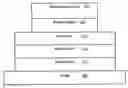
FIG. 1 is a perspective view of a circuit package, without a lid, according to one embodiment of the present invention; and
FIG. 2 is a perspective view of the circuit package of FIG. 1 with a lid attached thereto; and
FIG. 3 is a diagrammatic elevation view of a circuit package in accordance with the invention illustrating the several layers.
DETAILED DESCRIPTION OF THE INVENTION
One embodiment of a microcircuit package in accordance with the invention is shown in FIG. 1. The circuit package 100 includes a flange 102, a frame 104 and two leads 106 and 108 extending from respective sides of the package. The frame 104 electrically insulates the leads 106 and 108 from the flange 102 and from each other. A semiconductor die 110 is attached to a die attach area 112 within the area defined by the frame 104. The die 110 is attached to the die attach area 112 by a eutectic or other appropriate solder 114. In the illustrated embodiment only one die is shown, although two or more dies can typically be attached to the die attach area 112 in accordance with application and user requirements.
The eutectic solder 114 electrically bonds the die 110 to the confronting surface of the flange 102. The leads 106 and 108 are connected to contact areas of the die 110 by wire bonded leads 120 and 122. A lid 200 is attached to the confronting periphery of the frame 104 to enclose the die, as illustrated in FIG. 2.
The flange 102 forms a base to which other parts of the circuit package are attached, and also serves as a heat sink to conduct heat from the one or more semiconductor dies mounted in the package. The flange is preferably made of copper or a high copper alloy to provide high electrical and thermal conductivity. The frame 104 is made of an injunction molded thermoplastic and is molded to the flange 102 and to the leads 106 and 108.
The frame material is preferably a liquid crystal polymer (LCP) that can withstand die attach temperatures which typically are 280-330° C. for AuSn soldering, or 390-420° C. for AuSi soldering. Preferable high temperature LCP frame materials are further described, for example, in Applicant's prior U.S. Pat. No. 7,053,299. The high temperature polymeric material can have a composition which includes one of the following chemical groups: hydroquinine (HQ), 4,4 bisphenol (BP), bis (4-hydroxylphenyl ether) (POP), terephalic acid (TPA), 2,6 naphalene dicarboxylic acid (NPA), 4,4 benzoic acid (BB), 4-hydrosybenzoic acid (HBA), 6-hydroxy-2-naptholic acid (HNA).
The leads 106 and 108 are preferably made of an alloy of copper which may be of many alternative compositions such as those described in the aforesaid U.S. Pat. No. 7,053,299. The copper alloys include those known under the UNS designations C19400, C15100, C19500, C19700, C50710, C19210, C19520, C18070, C19010, C70250, EFTEC-64T, KLF-25 and MF224.
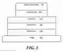
In accordance with the present invention, a ductile layer is provided between the flange and the die attach. The multi-layer structure of a preferred embodiment is illustrated in FIG. 3. Referring to FIG. 3, the microcircuit package comprises a flange or substrate 200 of copper or copper alloy, having a ductile layer 210, typically of copper or silver, applied on a surface of the flange. A barrier layer 212 of nickel or nickel cobalt is applied over the ductile layer, and a gold layer 214 is applied over the nickel layer. A eutectic solder 216, typically of gold-tin (AuSn), gold-silicon (AuSi), or gold-germanium (AuGe)is applied over the gold layer, and one or more semiconductor dies 218 are attached to the eutectic solder. The semiconductor dies can be fabricated from materials such as silicon, gallium arsenide, gallium nitride or any other suitable semiconductor material.
The flange 200 typically has a thickness in the range of about 0.040-0.060 inches. The ductile layer 210 has a thickness in the range of about 100-500 micro-inches. The barrier layer 212 has a thickness in the range of about 100-200 micro-inches. The semiconductor dies 218 typically have a thickness in the range of about 0.002-0.010 inches. The thickness of the gold layer 214 will depend upon the type of eutectic solder employed. For gold-tin (AuSn) solder, the gold layer on the flange has a thickness in the range of about 30-50 micro-inches.
In another embodiment, for a package having gold-tin solder, a gold layer of about 25 micro-inches is applied over a palladium layer of about 5 micro-inches.
When a eutectic solder of gold-silicon (Ausi) or gold germanium (AuGe) is used, the gold layer has a thickness in the range of about 100-200 micro-inches.
The eutectic solder can be a lead-free solder such as tin-silver-copper (SnAgCu), tin-silver (SnAg), antimony-tin (SbSn), tin-zinc (SnZn), bismuth (Bi) and tin-indium (SnIn). For use with these lead-free solders, a layer of nickel is applied at a thickness of about 150 micro-inches over the ductile layer. Optionally, a “flash” coating of about 5 micro-inches of gold can be applied over the nickel layer to prevent oxidation of the nickel.
The ductile layer 210 can be copper, silver, or an alloy of copper and silver, and the ductile layer can be provided in several different ways such as by plating, cladding, evaporation, and sputtering. The ductile layer has hardness less than about 80 Knoop and a thickness in the range of about 100 to 1000 micro-inches, and preferably in the range of about 100 to 500 micro-inches.
For efficient manufacturing, the flange 200 can be made of a harder form of copper or other suitable material, which is more resistant to damage during manufacturing such as scratches, nicks, and the like. A preferred hardness is greater than 80 Knoop and preferably in the range of about 85-100 Rockwell F.
In a preferred embodiment the flange 10 can be made of a copper zirconium alloy (CDA 151) which has hardness in the intended range of 85-100 Rockwell F.
As a comparison, the widely used oxygen-free copper (CDA101/102) is very soft and is prone to nicks, scratches and the like and has an annealing temperature of about 350° C. In contrast, CDA 151 copper has an annealing temperature greater than 500° C. and a significantly greater hardness. Thus, the harder flange material is more stable and suitable for efficient manufacturing processes.
The invention is not to be limited by what has been particularly shown and described but is to encompass the full spirit and scope of the claims.
Claims
What is claimed is:1. A microcircuit package comprising:
a substrate having a first surface;
a layer of ductile material having a first surface and a second surface, the first surface of the layer attached to the first surface of the substrate;
a barrier layer having a first surface and a second surface, the first surface of the barrier layer attached to the second surface of the layer of ductile material;
a gold layer having a first surface and a second surface, the first surface of the gold layer attached to the second surface of the barrier layer;
a eutectic layer having a first surface and a second surface, the first surface of the eutectic layer attached to the second surface of the gold layer; and
a semiconductor device attached to the second surface of the eutectic layer.
2. The microcircuit package of claim 1 wherein the layer of ductile material is silver, copper or an alloy of silver and copper.
3. The microcircuit package of claim 2 wherein the layer of ductile material is electroplated onto the first surface of the substrate.
4. The microcircuit package of claim 2 wherein the layer of ductile material is applied to the first surface of the substrate by plating, cladding, evaporation or sputtering.
5. The microcircuit package of claim 2 wherein the layer of ductile material has a hardness of less than about 80 Knoop and a thickness of about 100-1000 micro-inches, and preferably about 100-500 micro-inches.
6. The microcircuit package of claim 5 wherein the barrier layer is nickel or nickel cobalt.
7. The microcircuit package of claim 5 wherein the eutectic layer is gold-tin (AuSn), gold silicon (AuSi) solder, or gold-germanium (AuGe).
8. The microcircuit package of claim 5 wherein the eutectic layer is a lead-free solder.
9. The microcircuit package of claim 8 wherein the lead-free solder is selected from the group consisting of Sn—Ag—Cu, SnAg, SbSn, SnZn, Bi and SnIn.
10. The microcircuit package of claim 5 wherein the eutectic layer is a solder with a eutectic temperature of about 250° C. or higher.
11. The microcircuit package of claim 5 wherein the substrate is a copper zirconium alloy.
12. The microcircuit package of claim 5 wherein the substrate has a hardness of greater than about 80 Knoop and preferably in the range of about 85-100 Rockwell F.
13. The microcircuit package of claim 5 wherein the gold layer has a thickness of about 30-50 micro-inches.
14. The microcircuit package of claim 1 which also has a dielectric material attached which has a CTE in the range of 12-25 ppm/° C.
15. The microcircuit package of claim 14, where the dielectric material is a high temperature polymeric material that has a composition which includes a chemical group selected from the chemical groups consisting of: hydroquinine (HQ), 4,4 bisphenol (BP), bis (4-hydroxylphenyl ether) (POP), terephalic acid (TPA), 2,6 naphalene dicarboxylic acid (NPA), 4,4 benzoic acid (BB), 4-hydrosybenzoic acid (HBA), 6-hydroxy-2-naptholic acid (HNA).
Images & Drawings included:
Sources:
- United States Patent and Trademark Office - verify current appl. status at the USPTO↗
Recent applications in this class:
- » 20250246490 2025-07-31
Electronic Component With Reduced Inductance - » 20250210425 2025-06-26
METAL CORE SUBSTRATE AND METHOD OF PRODUCING THE METAL CORE SUBSTRATE - » 20250118607 2025-04-10
SUBSTRATE FOR POWER SEMICONDUCTOR PACKAGING AND A PACKAGE CONTAINING SUCH SUBSTRATE - » 20240371712 2024-11-07
METHOD OF IMPROVING PACKAGE CREEPAGE DISTANCE - » 20240332099 2024-10-03
SEMICONDUCTOR PACKAGE HAVING AN ELECTRICALLY INSULATING CORE WITH EXPOSED GLASS FIBRES - » 20240321655 2024-09-26
SEMICONDUCTOR MODULE - » 20240243022 2024-07-18
POWER SEMICONDUCTOR DEVICE, METHOD FOR PREPARING POWER SEMICONDUCTOR DEVICE, AND ELECTRONIC APPARATUS - » 20240222209 2024-07-04
Composite substrate and method of producing the composite substrate, and semiconductor device comprising the composite substrate - » 20240112968 2024-04-04
ANODIC ALUMINUM OXIDE FILM-BASED INTERPOSER FOR ELECTRICAL CONNECTION AND MANUFACTURING METHOD THEREFOR, SEMICONDUCTOR PACKAGE AND MANUFACTURING METHOD THEREFOR, MULTI-STACKED SEMICONDUCTOR DEVICE AND MANUFACTURING METHOD THEREFOR, DISPLAY AND MANUFACTURING METHOD THEREFOR - » 20240087970 2024-03-14
SEMICONDUCTOR DEVICE AND METHOD OF MANUFACTURING SEMICONDUCTOR DEVICE
Recent applications for this Assignee:
- » 20110064881 2011-03-17
Plastic electronic component package - » 20090295036 2009-12-03
Ultra high-temperature plastic package and method of manufacture - » 20050012080 2005-01-20
Thermoplastic material