Reducing formation of oxide on solder
US20120111925A1
2012-05-10
13/231,749
2011-09-13
✅ Patent granted
US 8,844,793 B2
2014-09-30
-
-
Kiley Stoner
Daly, Crowley, Mofford & Durkee, LLP
2031-09-13
Abstract:
In certain embodiments, a system includes a deposition system and a plasma/bonding system. The deposition system deposits a solder outwardly from a substrate of a number of substrates. The plasma/bonding system comprises a plasma system configured to plasma clean the substrate and a bonding system configured to bond the substrates. The plasma/bonding system at least reduces reoxidation of the solder. In certain embodiments, a method comprises depositing solder outwardly from a substrate, removing metal oxide from the substrate, and depositing a capping layer outwardly from the substrate to at least reduce reoxidation of the solder.
Inventors:
- Buu Diep 13 🇺🇸 Murphy, TX, United States
- Roland W. Gooch 26 🇺🇸 Dallas, TX, United States
- Thomas A. Kocian 14 🇺🇸 Dallas, TX, United States
Assignee:
- RAYTHEON COMPANY 5,596 🇺🇸 Waltham, MA, United States
Applicant:
Interested in similar patents?
Get notified when new applications in this technology area are published.
Classification:
B23K1/203 » CPC further
Soldering, e.g. brazing, or unsoldering; Preliminary treatment of work or areas to be soldered, e.g. in respect of a galvanic coating Fluxing, i.e. applying flux onto surfaces
B23K2101/40 » CPC further
Articles made by soldering, welding or cutting; Electric or electronic devices Semiconductor devices
H01L21/67173 » CPC main
Processes or apparatus adapted for the manufacture or treatment of semiconductor or solid state devices or of parts thereof; Apparatus specially adapted for handling semiconductor or electric solid state devices during manufacture or treatment thereof; Apparatus specially adapted for handling wafers during manufacture or treatment of semiconductor or electric solid state devices or components ; Apparatus not specifically provided for elsewhere; Apparatus not specifically provided for elsewhere; Apparatus for manufacture or treatment; Apparatus for manufacturing or treating in a plurality of work-stations characterized by the layout of the process chambers in-line arrangement
H01L2224/83 » CPC further
Indexing scheme for arrangements for connecting or disconnecting semiconductor or solid-state bodies and methods related thereto as covered by; Methods for connecting semiconductor or other solid state bodies using means for bonding being attached to, or being formed on, the surface to be connected using a layer connector
H01L2924/0105 » CPC further
Indexing scheme for arrangements or methods for connecting or disconnecting semiconductor or solid-state bodies as covered by; Chemical elements Tin [Sn]
H01L2224/7501 » CPC further
Indexing scheme for arrangements for connecting or disconnecting semiconductor or solid-state bodies and methods related thereto as covered by; Apparatus for manufacturing arrangements for connecting or disconnecting semiconductor or solid-state bodies and for methods related thereto; Apparatus for connecting with bump connectors or layer connectors Means for cleaning, e.g. brushes, for hydro blasting, for ultrasonic cleaning, for dry ice blasting, using gas-flow, by etching, by applying flux or plasma
H01L2924/1461 » CPC further
Indexing scheme for arrangements or methods for connecting or disconnecting semiconductor or solid-state bodies as covered by; Details of semiconductor or other solid state devices to be connected; Mixed devices MEMS
H01L2924/181 » CPC further
Indexing scheme for arrangements or methods for connecting or disconnecting semiconductor or solid-state bodies as covered by; Details of package parts other than the semiconductor or other solid state devices to be connected Encapsulation
H01L2924/14 » CPC further
Indexing scheme for arrangements or methods for connecting or disconnecting semiconductor or solid-state bodies as covered by; Details of semiconductor or other solid state devices to be connected; Device type Integrated circuits
H01L2924/00 » CPC further
Indexing scheme for arrangements or methods for connecting or disconnecting semiconductor or solid-state bodies as covered by
B23K31/02 IPC
Processes relevant to this subclass, specially adapted for particular articles or purposes, but not covered by only one of the preceding main groups relating to soldering or welding
B23K3/06 IPC
Tools, devices, or special appurtenances for soldering, e.g. brazing, or unsoldering, not specially adapted for particular methods Solder feeding devices; Solder melting pans
H01L2224/83815 » CPC further
Indexing scheme for arrangements for connecting or disconnecting semiconductor or solid-state bodies and methods related thereto as covered by; Methods for connecting semiconductor or other solid state bodies using means for bonding being attached to, or being formed on, the surface to be connected using a layer connector; Bonding techniques; Soldering or alloying Reflow soldering
H01L21/67092 » CPC further
Processes or apparatus adapted for the manufacture or treatment of semiconductor or solid state devices or of parts thereof; Apparatus specially adapted for handling semiconductor or electric solid state devices during manufacture or treatment thereof; Apparatus specially adapted for handling wafers during manufacture or treatment of semiconductor or electric solid state devices or components ; Apparatus not specifically provided for elsewhere; Apparatus not specifically provided for elsewhere; Apparatus for manufacture or treatment Apparatus for mechanical treatment
H01L2924/014 » CPC further
Indexing scheme for arrangements or methods for connecting or disconnecting semiconductor or solid-state bodies as covered by; Alloys Solder alloys
H01L2924/01029 » CPC further
Indexing scheme for arrangements or methods for connecting or disconnecting semiconductor or solid-state bodies as covered by; Chemical elements Copper [Cu]
H01L2224/75102 » CPC further
Indexing scheme for arrangements for connecting or disconnecting semiconductor or solid-state bodies and methods related thereto as covered by; Apparatus for manufacturing arrangements for connecting or disconnecting semiconductor or solid-state bodies and for methods related thereto; Apparatus for connecting with bump connectors or layer connectors; Means for controlling the bonding environment, e.g. valves, vacuum pumps; Chamber Vacuum chamber
H01L24/75 » CPC further
Arrangements for connecting or disconnecting semiconductor or solid-state bodies; Methods or apparatus related thereto; Apparatus for manufacturing arrangements for connecting or disconnecting semiconductor or solid-state bodies Apparatus for connecting with bump connectors or layer connectors
H01L2224/27826 » CPC further
Indexing scheme for arrangements for connecting or disconnecting semiconductor or solid-state bodies and methods related thereto as covered by; Means for bonding being attached to, or being formed on, the surface to be connected, e.g. chip-to-package, die-attach, "first-level" interconnects; Manufacturing methods related thereto; Layer connectors, e.g. plate connectors, solder or adhesive layers; Manufacturing methods related thereto; Manufacturing methods; Post-treatment of the layer connector; Applying permanent coating, e.g. in-situ coating Physical vapour deposition [PVD], e.g. evaporation, or sputtering
H01L2224/2781 » CPC further
Indexing scheme for arrangements for connecting or disconnecting semiconductor or solid-state bodies and methods related thereto as covered by; Means for bonding being attached to, or being formed on, the surface to be connected, e.g. chip-to-package, die-attach, "first-level" interconnects; Manufacturing methods related thereto; Layer connectors, e.g. plate connectors, solder or adhesive layers; Manufacturing methods related thereto; Manufacturing methods; Post-treatment of the layer connector Cleaning, e.g. oxide removal step, desmearing
H01L2224/94 » CPC further
Indexing scheme for arrangements for connecting or disconnecting semiconductor or solid-state bodies and methods related thereto as covered by; Batch processes at wafer-level, i.e. with connecting carried out on a wafer comprising a plurality of undiced individual devices
H01L21/67207 » CPC further
Processes or apparatus adapted for the manufacture or treatment of semiconductor or solid state devices or of parts thereof; Apparatus specially adapted for handling semiconductor or electric solid state devices during manufacture or treatment thereof; Apparatus specially adapted for handling wafers during manufacture or treatment of semiconductor or electric solid state devices or components ; Apparatus not specifically provided for elsewhere; Apparatus not specifically provided for elsewhere; Apparatus for manufacture or treatment; Apparatus for manufacturing or treating in a plurality of work-stations comprising a chamber adapted to a particular process
H01L24/83 » CPC further
Arrangements for connecting or disconnecting semiconductor or solid-state bodies; Methods or apparatus related thereto; Methods for connecting semiconductor or other solid state bodies using means for bonding being attached to, or being formed on, the surface to be connected using a layer connector
H01L2224/83013 » CPC further
Indexing scheme for arrangements for connecting or disconnecting semiconductor or solid-state bodies and methods related thereto as covered by; Methods for connecting semiconductor or other solid state bodies using means for bonding being attached to, or being formed on, the surface to be connected using a layer connector; Pre-treatment of the layer connector or the bonding area; Cleaning the layer connector, e.g. oxide removal step, desmearing Plasma cleaning
B23K3/047 » CPC further
Tools, devices, or special appurtenances for soldering, e.g. brazing, or unsoldering, not specially adapted for particular methods; Heating appliances electric
H01L24/742 » CPC further
Arrangements for connecting or disconnecting semiconductor or solid-state bodies; Methods or apparatus related thereto; Apparatus for manufacturing arrangements for connecting or disconnecting semiconductor or solid-state bodies; Apparatus for manufacturing means for bonding, e.g. connectors Apparatus for manufacturing bump connectors
H01L2224/2745 » CPC further
Indexing scheme for arrangements for connecting or disconnecting semiconductor or solid-state bodies and methods related thereto as covered by; Means for bonding being attached to, or being formed on, the surface to be connected, e.g. chip-to-package, die-attach, "first-level" interconnects; Manufacturing methods related thereto; Layer connectors, e.g. plate connectors, solder or adhesive layers; Manufacturing methods related thereto; Manufacturing methods by blanket deposition of the material of the layer connector in gaseous form Physical vapour deposition [PVD], e.g. evaporation, or sputtering
H01L2224/27318 » CPC further
Indexing scheme for arrangements for connecting or disconnecting semiconductor or solid-state bodies and methods related thereto as covered by; Means for bonding being attached to, or being formed on, the surface to be connected, e.g. chip-to-package, die-attach, "first-level" interconnects; Manufacturing methods related thereto; Layer connectors, e.g. plate connectors, solder or adhesive layers; Manufacturing methods related thereto; Manufacturing methods by local deposition of the material of the layer connector in liquid form by dispensing droplets
B23K1/206 » CPC main
Soldering, e.g. brazing, or unsoldering; Preliminary treatment of work or areas to be soldered, e.g. in respect of a galvanic coating Cleaning
H01L2224/2746 » CPC further
Indexing scheme for arrangements for connecting or disconnecting semiconductor or solid-state bodies and methods related thereto as covered by; Means for bonding being attached to, or being formed on, the surface to be connected, e.g. chip-to-package, die-attach, "first-level" interconnects; Manufacturing methods related thereto; Layer connectors, e.g. plate connectors, solder or adhesive layers; Manufacturing methods related thereto; Manufacturing methods by blanket deposition of the material of the layer connector Plating
B23K1/008 » CPC further
Soldering, e.g. brazing, or unsoldering Soldering within a furnace
H01L2224/0401 » CPC further
Indexing scheme for arrangements for connecting or disconnecting semiconductor or solid-state bodies and methods related thereto as covered by; Means for bonding being attached to, or being formed on, the surface to be connected, e.g. chip-to-package, die-attach, "first-level" interconnects; Manufacturing methods related thereto; Bonding areas; Manufacturing methods related thereto; Structure, shape, material or disposition of the bonding areas prior to the connecting process Bonding areas specifically adapted for bump connectors, e.g. under bump metallisation [UBM]
H01L24/27 » CPC further
Arrangements for connecting or disconnecting semiconductor or solid-state bodies; Methods or apparatus related thereto; Means for bonding being attached to, or being formed on, the surface to be connected, e.g. chip-to-package, die-attach, "first-level" interconnects; Manufacturing methods related thereto; Layer connectors, e.g. plate connectors, solder or adhesive layers; Manufacturing methods related thereto Manufacturing methods
B23K1/0016 » CPC further
Soldering, e.g. brazing, or unsoldering specially adapted for particular articles or work Brazing of electronic components
H01L2224/834 » CPC further
Indexing scheme for arrangements for connecting or disconnecting semiconductor or solid-state bodies and methods related thereto as covered by; Methods for connecting semiconductor or other solid state bodies using means for bonding being attached to, or being formed on, the surface to be connected using a layer connector; Bonding interfaces outside the semiconductor or solid-state body; Material with a principal constituent of the material being a metal or a metalloid, e.g. boron [B], silicon [Si], germanium [Ge], arsenic [As], antimony [Sb], tellurium [Te] and polonium [Po], and alloys thereof
H01L24/29 » CPC further
Arrangements for connecting or disconnecting semiconductor or solid-state bodies; Methods or apparatus related thereto; Means for bonding being attached to, or being formed on, the surface to be connected, e.g. chip-to-package, die-attach, "first-level" interconnects; Manufacturing methods related thereto; Layer connectors, e.g. plate connectors, solder or adhesive layers; Manufacturing methods related thereto; Structure, shape, material or disposition of the layer connectors prior to the connecting process of an individual layer connector
H01L24/94 » CPC further
Arrangements for connecting or disconnecting semiconductor or solid-state bodies; Methods or apparatus related thereto; Batch processes at wafer-level, i.e. with connecting carried out on a wafer comprising a plurality of undiced individual devices
B23K3/08 » CPC further
Tools, devices, or special appurtenances for soldering, e.g. brazing, or unsoldering, not specially adapted for particular methods Auxiliary devices therefor
B23K37/00 IPC
Auxiliary devices or processes, not specially adapted to a procedure covered by only one of the preceding main groups
H01L21/67 IPC
Processes or apparatus adapted for the manufacture or treatment of semiconductor or solid state devices or of parts thereof Apparatus specially adapted for handling semiconductor or electric solid state devices during manufacture or treatment thereof; Apparatus specially adapted for handling wafers during manufacture or treatment of semiconductor or electric solid state devices or components ; Apparatus not specifically provided for elsewhere
H01L23/00 IPC
Details of semiconductor or other solid state devices
B23K1/20 » CPC further
Soldering, e.g. brazing, or unsoldering Preliminary treatment of work or areas to be soldered, e.g. in respect of a galvanic coating
B23K1/00 IPC
Soldering, e.g. brazing, or unsoldering
B23K1/00 IPC
Soldering, e.g. brazing, or unsoldering
H01L2224/83201 » CPC further
Indexing scheme for arrangements for connecting or disconnecting semiconductor or solid-state bodies and methods related thereto as covered by; Methods for connecting semiconductor or other solid state bodies using means for bonding being attached to, or being formed on, the surface to be connected using a layer connector; Applying energy for connecting Compression bonding
H01L2224/27334 » CPC further
Indexing scheme for arrangements for connecting or disconnecting semiconductor or solid-state bodies and methods related thereto as covered by; Means for bonding being attached to, or being formed on, the surface to be connected, e.g. chip-to-package, die-attach, "first-level" interconnects; Manufacturing methods related thereto; Layer connectors, e.g. plate connectors, solder or adhesive layers; Manufacturing methods related thereto; Manufacturing methods by local deposition of the material of the layer connector in solid form using preformed layer
Description
RELATED APPLICATION
This application claims benefit under 35 U.S.C. §119(e) of U.S. Provisional Application Ser. No. 61/410,454, entitled “Plasma Removal of Metal Oxide,” Attorney's Docket 004578.2146, filed Nov. 5, 2010, by Buu Diep et al., which is incorporated herein by reference.
BACKGROUND
In the electronics packaging industry, plasma cleaning with a gas mixture (such as an H2 mixture) may be performed to remove oxide formation.
SUMMARY OF THE DISCLOSURE
In accordance with the present invention, disadvantages and problems associated with previous techniques for reducing formation of metal oxides on solder may be reduced or eliminated.
In certain embodiments, a system includes a deposition system and a plasma/bonding system. The deposition system deposits a solder outwardly from a substrate of a number of substrates. The plasma/bonding system comprises a plasma system configured to plasma clean the substrate and a bonding system configured to bond the substrates. The plasma/bonding system at least reduces reoxidation of the solder.
In certain embodiments, a method comprises depositing solder outwardly from a substrate, removing metal oxide from the substrate, and depositing a capping layer outwardly from the substrate to at least reduce reoxidation of the solder.
Certain embodiments of the invention may provide one or more technical advantages. A technical advantage of one embodiment may be that a plasma/bonding system may be used to at least reduce (or even prevent) formation of metal oxide. The system may plasma clean and then bond wafers without exposing the wafers to oxygen, which may at least reduce formation of metal oxide. A technical advantage of one embodiment may be that a capping layer may protect a wafer from exposure to oxygen, which may reduce formation of metal oxide.
Certain embodiments of the invention may include none, some, or all of the above technical advantages. One or more other technical advantages may be readily apparent to one skilled in the art from the figures, descriptions, and claims included herein.
BRIEF DESCRIPTION OF THE DRAWINGS
For a more complete understanding of the present invention and its features and advantages, reference is now made to the following description, taken in conjunction with the accompanying drawings, in which:
FIG. 1 illustrates an example of a system that may at least reduce reformation of metal oxides on a substrate;
FIGS. 2A through 2B illustrate examples of one or more chambers that may reduce reformation of metal oxides on a substrate;
FIG. 3 illustrates an example of a method that may reduce reformation of metal oxides on a substrate;
FIG. 4 illustrates an example a chamber that may reduce reformation of metal oxides on a substrate; and
FIG. 5 illustrates an example two chambers that may reduce reformation of metal oxides on a substrate.
DETAILED DESCRIPTION OF THE DRAWINGS
Embodiments of the present invention and its advantages are best understood by referring to FIGS. 1 through 4 of the drawings, like numerals being used for like and corresponding parts of the various drawings.
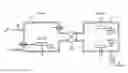
FIG. 1 illustrates an example of a system 10 that may at least reduce reformation of metal oxides on a substrate. System 10 may have one or more chambers designed to reduce reformation or may apply a capping layer that reduces reformation.
Certain solders oxidize in air and form a metal oxide (such as Sn oxide). The presence of oxides can cause problems that may prevent formation of a good bond line. For example, the oxides may yield formation of voids or may cause de-wetting of the solder during the bonding process. These problems can lead to yield loss or reliability problems.
Plasma clean with a gas mixture (such as an H2 mixture) may be performed to remove oxide formation. Oxide, however, may re-form as soon as the cleaned part is exposed to air. For example, for wafer level bonding using jetted solder, Sn is readily oxidized in air after the solder is jetted forming tin oxide.
In certain embodiments, system 10 may operate on a substrate, such as a wafer. A wafer may be a thin slice of semiconductor material, such as silicon crystal. A wafer may be used in the fabrication of integrated circuits and other microdevices, and may serve as the substrate for microelectronic devices disposed within and outwardly from the wafer. Substrates may have any suitable application, such as microelectromechanical systems (MEMS) devices or infrared (IR) detectors. For example, a first substrate with a base metal stack (such as a Ti/Pt/Au metal stack) and a second substrate with MEMS may be bonded together with solder.
In the illustrated example, system 10 comprises a printing system 20 (with a deposition system 26) and a plasma/bonding system 24. Deposition system 26 deposits a solder outwardly from at least one substrate of one or more substrates. Plasma/bonding system 24 comprises a plasma system and a bonding system. The plasma system plasma cleans at least one substrate, and the bonding system bonds substrates. Plasma/bonding system 24 at least reduces reformation of metal oxide on the solder (or reoxidation of the solder). Printing system 20 and plasma/bonding system 24 may be separated into district systems that each perform it own operations or may be combined into one system that performs one or more operations of both systems.
Printing system 26 may deposit solder on a substrate. In certain embodiments, printing system 20 may include a deposition system 26. Deposition system 26 deposits a solder outwardly from a substrate in any suitable manner. For example, solder may be deposited by solder-jetting. As another example, a solder preform, a specially designed shape of solder, may be used. Other example techniques include physical vapor deposition and plating.
Solder comprises a fusible metal alloy with a melting point in the range of 90 to 450 degree Celsius (190 to 840° F.) (such as 180 and 190° C. (360 and 370° F.)) that may be melted to join metallic surfaces. Solder may comprise any suitable combination of any suitable metals. Examples of metals include tin, lead, copper, silver, bismuth, indium, zinc, antimony, and traces of other metals. In certain examples, solder may comprise a gold-tin alloy, such as Au80Sn20.
In certain embodiments, printing system 20 may first form a pattern of photoresist that indicates areas to apply solder on a substrate. Deposition system 26 may then deposit solder as indicated by the areas.
Plasma/bonding system 24 plasma cleans substrates and bonds substrates together. Plasma/bonding system 24 may plasma clean in any suitable manner. In certain embodiments, plasma cleaning cleans substrates with an energetic plasma created from gas. Any suitable gas may be used, such as a gas comprising one or more of the following: hydrogen, nitrogen, argon, helium, or air. The plasma may be created by using high frequency voltages to ionize the low pressure gas. In the plasma, gas atoms are excited to higher energy states and ionized. The plasma activated atoms and ions behave like a molecular sandblast and break down organic contaminants. The contaminants are vaporized and removed.
Plasma/bonding system 24 may bond substrates in any suitable manner. In certain embodiments, plasma/bonding system 24 may align the substrates, one or more of which may have solder deposited on it. Plasma bonding system 24 may then apply pressure to one or more of the substrates to bond the substrates together.
Plasma/bonding system 24 at least reduces (and may even prevent) reformation of metal oxide on a substrate in any suitable manner. In certain embodiments, plasma/bonding system 24 may have one or more chambers designed to reduce exposure of the substrate to oxygen. A chamber may be an enclosure from which one or more gasses have been removed. For example, a chamber may be a vacuum chamber with a low pressure, such as less than or 10 to 20 pascal (Pa). As another example, a chamber may use one gas to push out another gas. For example, a nitrogen chamber may use nitrogen gas to push out oxygen gas to yield a low concentration of oxygen, such as less than 1 parts per million (ppm).
A chamber may have one or more ports, covered with vacuum flanges, to allow instruments or windows to be installed in the walls of the chamber. The chambers may be arranged in any suitable manner. Examples of plasma/bonding systems 24 are described in more detail with reference to FIGS. 2A through 2C.
FIG. 2A illustrates an example of plasma/bonding system 24 that comprises a plasma/bonding chamber 30. Substrates are plasma cleaned and bonded in plasma/bonding chamber 30 such that the solder is not exposed to air after metal oxide removal and prior to bonding. For example, a plasma system may be integrated with a bonding system in plasma/bonding chamber 30.
FIG. 2B illustrates an example of plasma/bonding system 24 that comprises a plasma chamber 34, a load-lock module 36, and a bonding chamber 38. A substrate is plasma cleaned in plasma chamber 34, and substrates are bonded in bonding chamber 38. In certain embodiments, plasma chamber 34 can be coupled to bonding chamber 38 via load-lock module 36 configured to couple chambers under a substantial vacuum. In certain embodiments, plasma chamber 34 can be coupled to bonding chamber 38 under a substantial vacuum without aid of load-lock module 36.
FIG. 2C illustrates an example of plasma/bonding system 24 that comprises a chamber 40. Plasma chamber 34 and bonding chamber 38 are disposed within chamber 40. In certain embodiments, chamber 40 may be a nitrogen chamber configured to use nitrogen gas to push oxygen gas outside of the nitrogen chamber. In certain embodiments, chamber 40 may be a vacuum chamber within which there is a substantial vacuum.
In certain embodiments, plasma/bonding system 24 of FIG. 1 may use a capping layer to reduce reformation of metal oxide on a substrate. System 10 (for example, printing system 20 and/or plasma/bonding system 24) may then plasma clean the substrate and then apply a capping layer resistant to oxidation to the substrate. System 10 may then etch and clean the substrate. An example of these embodiments is described in more detail with reference to FIG. 3.
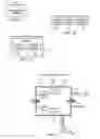
FIG. 3 illustrates an example of a method that may reduce reformation of metal oxides on a substrate. The method starts at step 210, where photolithography may be performed on the substrate to yield a patterned metal layer on the substrate. The substrate may be patterned with photoresist at step 214. The photoresist pattern may indicate areas where solder should be placed. For example, solder may be placed in areas around a sealed area.
Solder is deposited outwardly from the substrate at step 218. A gold layer is depositing outwardly from the substrate at step 219. The solder may be deposited by deposition system 26 in areas indicated by the photoresist pattern. The metal oxide is removed from the substrate at step 220. The metal oxide may be removed in any suitable manner, for example, by plasma cleaning or sputter etch. For example, the surface of the solder may be bombarded by energetic ions to removes all or substantially all of the oxide from the solder.
A capping layer is applied outwardly from the substrate at step 224. The capping layer may comprise a capping material that is resistant to oxidation, such as gold. Applying the capping layer right after removal of the metal oxide and prior to any exposure of the substrate to oxygen may prevent reformation of metal oxide.
The capping layer may be applied in any suitable manner. For example, physical vapor deposition (PVD) may be used to deposit the capping layer by condensation of a vaporized form of the capping material. PVD uses physical methods, such as plasma sputter bombardment or high temperature vacuum evaporation, to deposit material. In sputter deposition, capping material is sputtered, or ejected, from a source and deposited outwardly from the substrate. In evaporation deposition, capping material is evaporated in a vacuum, which allows the vapor particles to travel directly to the substrate. The vapor particles then condense and are deposited outwardly from the substrate. After the capping layer is applied, the capping layer may protect the substrate from oxidation and substrate may be exposed to the atmosphere. In the final soldering process, the capping layer may be incorporated into the solder at the bond line. In certain embodiments, the composition of the solder may be adjusted to compensate for the gold added to the solder by the gold layer.
Photoresist and excess gold are removed at step 226. The surface is cleaned with O2 plasma at step 228. The substrate is aligned with another substrate at step 230. The substrates are bonded at step 234. The method then ends.
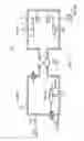
FIG. 4 illustrates an example of a chamber 30 of a plasma/bonding system 50 that may reduce reformation of metal oxides on a substrate. In the example, plasma/bonding system 50 comprises a plasma/bonding chamber 30 with a gas input 60 for plasma gas, electrodes 62 for plasma generation, a vacuum pump 64 that creates a vacuum in chamber 30, a support 66 that supports wafers, and a bonding plate 68 that bonds wafers.
FIG. 5 illustrates an example of two chambers 34 and 38 of a plasma/bonding system 52 that may reduce reformation of metal oxides on a substrate. In the example, plasma/bonding system 52 comprises a plasma chamber 34, a load-lock module 36, and a bonding chamber 38. Plasma chamber 34 has gas input 60 for plasma gas, electrodes 62 for plasma generation, and support 66 that supports wafers. Load-lock module 36 comprises a valve. Bonding chamber 38 has bonding plates 68 that bond wafers and vacuum pump 64 that creates a vacuum in chambers 34 and 38. Vacuum pump 64 may be placed in any suitable location of system 52, such as at plasma chamber 34 or load-lock module 36.
Modifications, additions, or omissions may be made to the systems and apparatuses disclosed herein without departing from the scope of the invention. The components of the systems and apparatuses may be integrated or separated. Moreover, the operations of the systems and apparatuses may be performed by more, fewer, or other components. Additionally, operations of the systems and apparatuses may be performed using any suitable logic comprising software, hardware, and/or other logic. As used in this document, “each” refers to each member of a set or each member of a subset of a set.
Modifications, additions, or omissions may be made to the methods disclosed herein without departing from the scope of the invention. The methods may include more, fewer, or other steps. Additionally, steps may be performed in any suitable order.
A component of the systems and apparatuses disclosed herein may include an interface, logic, memory, and/or other suitable element. An interface receives input, sends output, processes the input and/or output, and/or performs other suitable operation. An interface may comprise hardware and/or software.
Logic performs the operations of the component, for example, executes instructions to generate output from input. Logic may include hardware, software, and/or other logic. Logic may be encoded in one or more tangible media and may perform operations when executed by a computer. Certain logic, such as a processor, may manage the operation of a component. Examples of a processor include one or more computers, one or more microprocessors, one or more applications, and/or other logic.
In particular embodiments, the operations of the embodiments may be performed by one or more computer readable media encoded with a computer program, software, computer executable instructions, and/or instructions capable of being executed by a computer. In particular embodiments, the operations of the embodiments may be performed by one or more computer readable media storing, embodied with, and/or encoded with a computer program and/or having a stored and/or an encoded computer program.
A memory stores information. A memory may comprise one or more non-transitory, tangible, computer-readable, and/or computer-executable storage media. Examples of memory include computer memory (for example, Random Access Memory (RAM) or Read Only Memory (ROM)), mass storage media (for example, a hard disk), removable storage media (for example, a Compact Disk (CD) or a Digital Video Disk (DVD)), database and/or network storage (for example, a server), and/or other computer-readable medium.
Although this disclosure has been described in terms of certain embodiments, alterations and permutations of the embodiments will be apparent to those skilled in the art. Accordingly, the above description of the embodiments does not constrain this disclosure. Other changes, substitutions, and alterations are possible without departing from the spirit and scope of this disclosure, as defined by the following claims.
Claims
What is claimed is:1. A system comprising:
a deposition system configured to deposit a solder outwardly from at least one substrate of a plurality of substrates; and
a plasma/bonding system comprising:
a plasma system configured to plasma clean the at least one substrate; and
a bonding system configured to bond the plurality of substrates, the plasma/bonding system configured to at least reduce reoxidation of the solder.
2. The system of claim 1, the plasma/bonding system comprising:
a chamber in which the at least one substrate is plasma cleaned and the plurality of substrates are bonded.
3. The system of claim 1, the plasma/bonding system comprising:
a plasma chamber in which the at least one substrate is plasma cleaned; and
a bonding chamber in which the plurality of substrates are bonded, the bonding chamber coupled to the plasma chamber.
4. The system of claim 1, the plasma/bonding system comprising:
a plasma chamber in which the at least one substrate is plasma cleaned;
a bonding chamber in which the plurality of substrates are bonded; and
a load-lock module configured to couple the plasma chamber and the bonding chamber under a substantial vacuum.
5. The system of claim 1, the plasma/bonding system comprising:
a vacuum chamber within which there is a substantial vacuum;
a plasma chamber disposed within the vacuum chamber and in which the at least one substrate is plasma cleaned; and
a bonding chamber disposed within the vacuum chamber and in which the plurality of substrates are bonded.
6. The system of claim 1, the plasma/bonding system comprising:
a nitrogen chamber configured to use nitrogen gas to push oxygen gas outside of the nitrogen chamber;
a plasma chamber disposed within the nitrogen chamber and in which the at least one substrate is plasma cleaned; and
a bonding chamber disposed within the nitrogen chamber and in which the plurality of substrates are bonded.
7. The system of claim 1, the plasma/bonding system configured to:
a vacuum chamber within which there is a substantial vacuum;
a plasma chamber disposed within the vacuum chamber and in which the at least one substrate is plasma cleaned;
a bonding chamber disposed within the vacuum chamber and in which the plurality of substrates are bonded; and
a module configured to couple the plasma chamber and the bonding chamber.
8. A method comprising:
depositing a solder outwardly from at least one substrate of a plurality of substrates;
plasma cleaning the at least one substrate;
at least reducing reoxidation of the solder; and
bonding the plurality of substrates.
9. The method of claim 8, the at least reducing reoxidation of the solder comprising:
plasma cleaning the at least one substrate in a chamber; and
bonding the plurality of substrates in the chamber.
10. The method of claim 8, the at least reducing reoxidation of the solder comprising:
plasma cleaning the at least one substrate in a plasma chamber; and
bonding the plurality of substrates in a bonding chamber coupled to the plasma chamber.
11. The method of claim 8, the at least reducing reoxidation of the solder comprising:
plasma cleaning the at least one substrate in a plasma chamber;
transporting the at least one substrate to a bonding chamber through a load-lock module coupling the plasma chamber and the bonding chamber under a substantial vacuum; and
bonding the plurality of substrates in the bonding chamber.
12. The method of claim 8, the at least reducing reoxidation of the solder comprising:
plasma cleaning the at least one substrate in a plasma chamber disposed within a vacuum chamber within which there is a substantial vacuum; and
bonding the plurality of substrates in a bonding chamber disposed within the vacuum chamber.
13. The method of claim 8, the at least reducing reoxidation of the solder comprising:
plasma cleaning the at least one substrate in a plasma chamber disposed within a nitrogen chamber configured to use nitrogen gas to push oxygen gas outside of the nitrogen chamber; and
bonding the plurality of substrates in a bonding chamber disposed within the nitrogen chamber.
14. A method comprising:
depositing solder outwardly from a first substrate;
removing metal oxide from the first substrate; and
depositing a capping layer outwardly from the first substrate to at least reduce reoxidation of the solder.
15. The method of claim 7, further comprising:
bonding the first substrate and a second substrate.
16. The method of claim 7, further comprising:
allowing the first substrate to be exposed to atmosphere prior to bonding the first substrate and a second substrate.
17. The method of claim 7, the capping layer comprising gold.
18. A system comprising:
a deposition system configured to deposit a solder outwardly from a first substrate; and
a plasma/bonding system configured to:
remove metal oxide from the first substrate; and
deposit a capping layer outwardly from the first substrate to at least reduce reoxidation of the solder.
19. The system of claim 18, the plasma/bonding system configured to:
bond the first substrate and a second substrate.
20. The system of claim 18, the plasma/bonding system configured to:
allow the first substrate to be exposed to atmosphere prior to bonding the first substrate and a second substrate.
Images & Drawings included:

Sources:
- United States Patent and Trademark Office - verify current appl. status at the USPTO↗
Similar patent applications:
- » 20150076216
Reducing formation of oxide on solder
Recent applications in this class:
- » 20250091148 2025-03-20
SURFACE TREATMENT METHOD - » 20250050440 2025-02-13
METHOD OF CLEANING A BOTTOM PLATE - » 20240424588 2024-12-26
SYSTEM AND METHOD FOR DETERMINING WHETHER TO CLEAN A REFLOW OVEN - » 20240075546 2024-03-07
METHOD FOR JOINING, BY DIRECT BRAZING, A FIRST PART AND A SECOND PART, INCLUDING STEPS OF PREPARING THE SURFACE OF AT LEAST ONE OF THE PARTS - » 20180250762 2018-09-06
NARROW GAP PROCESSING - » 20180141144 2018-05-24
Method for cleaning an Electronic circuit board - » 20150076216 2015-03-19
Reducing formation of oxide on solder - » 20140263586 2014-09-18
Integrate rinse module in hybrid bonding platform - » 20130001277 2013-01-03
method for brazing a surface of a metallic substrate - » 20110094545 2011-04-28
Cleaning composition for removing lead-free solder flux and system for removing lead-free solder flux
Recent applications for this Assignee:
- » 20250167415 2025-05-22
ENHANCED BROADBAND RING RESONATOR FOR IMPROVED SPECTRAL SUPPRESSION - » 20250145355 2025-05-08
INTEGRATED CABLE PACKAGING, DEPLOYMENT AND STRUMMING MITIGATION SYSTEM - » 20250118501 2025-04-10
MICRO-ELECTROMECHANICAL SYSTEMS SWITCH WITH BEAM MOVEMENT ORTHOGONAL TO FORCE - » 20250116997 2025-04-10
PRODUCT IDENTIFICATION AND TRACKING SYSTEMS AND METHODS - » 20250116851 2025-04-10
REIMAGING LENS ASSEMBLY WITH ANGLED OPTIC - » 20250107006 2025-03-27
RF COVER LAYER - » 20250067792 2025-02-27
DEVICE FOR AND METHOD OF FREQUENCY TESTING PRINTED CIRCUIT BOARD UNDER THERMAL STRESS - » 20250062543 2025-02-20
CONFORMAL WAVEFRONT TRANSFORMER AND METHOD OF MAKING - » 20250035410 2025-01-30
TACTICAL HIGH POWER MICROWAVE ANTENNA PEDESTAL - » 20250027811 2025-01-23
ANTI-BLOOMING BUFFERED DIRECT INJECTION PIXELS