Semiconductor device and assembling method thereof
US20120161336A1
2012-06-28
13/089,289
2011-04-18
✅ Patent granted
US 8,415,795 B2
2013-04-09
-
-
David Zarneke
Jianq Chyun IP Office
2031-09-19
Abstract:
A semiconductor device and an assembling method thereof are provided. The semiconductor device includes a chip, a carrier, a plurality of first conductive elements and a plurality of second conductive elements. The chip has a plurality of first pads. The carrier has a plurality of second pads. The second pads correspond to the first pads. Each first conductive element is disposed between one of the first pads and one of the second pads. Each second conductive element is disposed between one of the first pads and one of the second pads. A volume ratio of intermetallic compound of the second conductive elements is greater than a volume ratio of intermetallic compound of the first conductive elements.
Inventors:
- Yu-Min Lin 10 🇹🇼 Changhua County, Taiwan
- Chau-Jie Zhan 2 🇹🇼 New Taipei City, Taiwan
- Su-Tsai Lu 16 🇹🇼 Hsinchu City, Taiwan
- Su-Tsai Lu 19 🇹🇼 Hsinchu, Taiwan
- Chau-Jie Zhan 2 🇹🇼 New Taipei, Taiwan
Assignee:
- INDUSTRIAL TECHNOLOGY RESEARCH INSTITUTE 7,890 🇹🇼 HSINCHU, Taiwan
Applicant:
Interested in similar patents?
Get notified when new applications in this technology area are published.
Classification:
H01L24/17 » CPC main
Arrangements for connecting or disconnecting semiconductor or solid-state bodies; Methods or apparatus related thereto; Means for bonding being attached to, or being formed on, the surface to be connected, e.g. chip-to-package, die-attach, "first-level" interconnects; Manufacturing methods related thereto; Bump connectors ; Manufacturing methods related thereto; Structure, shape, material or disposition of the bump connectors after the connecting process of a plurality of bump connectors
H01L23/345 » CPC further
Details of semiconductor or other solid state devices; Arrangements for cooling, heating, ventilating or temperature compensation ; Temperature sensing arrangements Arrangements for heating
H01L24/14 » CPC further
Arrangements for connecting or disconnecting semiconductor or solid-state bodies; Methods or apparatus related thereto; Means for bonding being attached to, or being formed on, the surface to be connected, e.g. chip-to-package, die-attach, "first-level" interconnects; Manufacturing methods related thereto; Bump connectors ; Manufacturing methods related thereto; Structure, shape, material or disposition of the bump connectors prior to the connecting process of a plurality of bump connectors
H01L24/81 » CPC further
Arrangements for connecting or disconnecting semiconductor or solid-state bodies; Methods or apparatus related thereto; Methods for connecting semiconductor or other solid state bodies using means for bonding being attached to, or being formed on, the surface to be connected using a bump connector
H01L21/563 » CPC further
Processes or apparatus adapted for the manufacture or treatment of semiconductor or solid state devices or of parts thereof; Manufacture or treatment of semiconductor devices or of parts thereof the devices having at least one potential-jump barrier or surface barrier, e.g. PN junction, depletion layer or carrier concentration layer; Assembly of semiconductor devices using processes or apparatus not provided for in a single one of the subgroups - , e.g. sealing of a cap to a base of a container; Encapsulations, e.g. encapsulation layers, coatings Encapsulation of active face of flip-chip device, e.g. underfilling or underencapsulation of flip-chip, encapsulation preform on chip or mounting substrate
H01L24/16 » CPC further
Arrangements for connecting or disconnecting semiconductor or solid-state bodies; Methods or apparatus related thereto; Means for bonding being attached to, or being formed on, the surface to be connected, e.g. chip-to-package, die-attach, "first-level" interconnects; Manufacturing methods related thereto; Bump connectors ; Manufacturing methods related thereto; Structure, shape, material or disposition of the bump connectors after the connecting process of an individual bump connector
H01L24/73 » CPC further
Arrangements for connecting or disconnecting semiconductor or solid-state bodies; Methods or apparatus related thereto Means for bonding being of different types provided for in two or more of groups , , , , , , ,
H01L24/92 » CPC further
Arrangements for connecting or disconnecting semiconductor or solid-state bodies; Methods or apparatus related thereto; Methods for connecting semiconductor or solid state bodies including different methods provided for in two or more of groups - Specific sequence of method steps
H01L25/0657 » CPC further
Assemblies consisting of a plurality of individual semiconductor or other solid state devices ; Multistep manufacturing processes thereof all the devices being of a type provided for in the same subgroup of groups - , e.g. assemblies of rectifier diodes the devices not having separate containers the devices being of a type provided for in group Stacked arrangements of devices
H01L2224/0401 » CPC further
Indexing scheme for arrangements for connecting or disconnecting semiconductor or solid-state bodies and methods related thereto as covered by; Means for bonding being attached to, or being formed on, the surface to be connected, e.g. chip-to-package, die-attach, "first-level" interconnects; Manufacturing methods related thereto; Bonding areas; Manufacturing methods related thereto; Structure, shape, material or disposition of the bonding areas prior to the connecting process Bonding areas specifically adapted for bump connectors, e.g. under bump metallisation [UBM]
H01L2224/14505 » CPC further
Indexing scheme for arrangements for connecting or disconnecting semiconductor or solid-state bodies and methods related thereto as covered by; Means for bonding being attached to, or being formed on, the surface to be connected, e.g. chip-to-package, die-attach, "first-level" interconnects; Manufacturing methods related thereto; Bump connectors; Manufacturing methods related thereto; Structure, shape, material or disposition of the bump connectors prior to the connecting process of a plurality of bump connectors; Material Bump connectors having different materials
H01L2224/17505 » CPC further
Indexing scheme for arrangements for connecting or disconnecting semiconductor or solid-state bodies and methods related thereto as covered by; Means for bonding being attached to, or being formed on, the surface to be connected, e.g. chip-to-package, die-attach, "first-level" interconnects; Manufacturing methods related thereto; Bump connectors; Manufacturing methods related thereto; Structure, shape, material or disposition of the bump connectors after the connecting process of a plurality of bump connectors; Material Bump connectors having different materials
H01L2224/81191 » CPC further
Indexing scheme for arrangements for connecting or disconnecting semiconductor or solid-state bodies and methods related thereto as covered by; Methods for connecting semiconductor or other solid state bodies using means for bonding being attached to, or being formed on, the surface to be connected using a bump connector; Arrangement of the bump connectors prior to mounting wherein the bump connectors are disposed only on the semiconductor or solid-state body
H01L2224/81193 » CPC further
Indexing scheme for arrangements for connecting or disconnecting semiconductor or solid-state bodies and methods related thereto as covered by; Methods for connecting semiconductor or other solid state bodies using means for bonding being attached to, or being formed on, the surface to be connected using a bump connector; Arrangement of the bump connectors prior to mounting wherein the bump connectors are disposed on both the semiconductor or solid-state body and another item or body to be connected to the semiconductor or solid-state body
H01L2224/81234 » CPC further
Indexing scheme for arrangements for connecting or disconnecting semiconductor or solid-state bodies and methods related thereto as covered by; Methods for connecting semiconductor or other solid state bodies using means for bonding being attached to, or being formed on, the surface to be connected using a bump connector; Applying energy for connecting using means for applying energy being within the device, e.g. integrated heater
H01L2224/8181 » CPC further
Indexing scheme for arrangements for connecting or disconnecting semiconductor or solid-state bodies and methods related thereto as covered by; Methods for connecting semiconductor or other solid state bodies using means for bonding being attached to, or being formed on, the surface to be connected using a bump connector; Bonding techniques; Soldering or alloying involving forming an intermetallic compound at the bonding interface
H01L2224/81815 » CPC further
Indexing scheme for arrangements for connecting or disconnecting semiconductor or solid-state bodies and methods related thereto as covered by; Methods for connecting semiconductor or other solid state bodies using means for bonding being attached to, or being formed on, the surface to be connected using a bump connector; Bonding techniques; Soldering or alloying Reflow soldering
H01L2224/81948 » CPC further
Indexing scheme for arrangements for connecting or disconnecting semiconductor or solid-state bodies and methods related thereto as covered by; Methods for connecting semiconductor or other solid state bodies using means for bonding being attached to, or being formed on, the surface to be connected using a bump connector; Post-treatment of the bump connector or bonding area Thermal treatments, e.g. annealing, controlled cooling
H01L2224/92125 » CPC further
Indexing scheme for arrangements for connecting or disconnecting semiconductor or solid-state bodies and methods related thereto as covered by; Methods for connecting semiconductor or solid state bodies including different methods provided for in two or more of groups - ; Specific sequence of method steps; Connecting a surface with connectors of different types; Sequential connecting processes the first connecting process involving a bump connector the second connecting process involving a layer connector
H01L2225/06513 » CPC further
Details relating to assemblies covered by the group but not provided for in its subgroups; All the devices being of a type provided for in the same subgroup of groups - the devices not having separate containers the devices being of a type provided for in group; Stacked arrangements of devices Bump or bump-like direct electrical connections between devices, e.g. flip-chip connection, solder bumps
H01L2225/06517 » CPC further
Details relating to assemblies covered by the group but not provided for in its subgroups; All the devices being of a type provided for in the same subgroup of groups - the devices not having separate containers the devices being of a type provided for in group; Stacked arrangements of devices Bump or bump-like direct electrical connections from device to substrate
H01L2924/01033 » CPC further
Indexing scheme for arrangements or methods for connecting or disconnecting semiconductor or solid-state bodies as covered by; Chemical elements Arsenic [As]
H01L2924/01079 » CPC further
Indexing scheme for arrangements or methods for connecting or disconnecting semiconductor or solid-state bodies as covered by; Chemical elements Gold [Au]
H01L2924/01327 » CPC further
Indexing scheme for arrangements or methods for connecting or disconnecting semiconductor or solid-state bodies as covered by; Alloys; Binary Alloys Intermediate phases, i.e. intermetallics compounds
H01L2924/014 » CPC further
Indexing scheme for arrangements or methods for connecting or disconnecting semiconductor or solid-state bodies as covered by; Alloys Solder alloys
H01L2924/01082 » CPC further
Indexing scheme for arrangements or methods for connecting or disconnecting semiconductor or solid-state bodies as covered by; Chemical elements Lead [Pb]
H01L2224/81224 » CPC further
Indexing scheme for arrangements for connecting or disconnecting semiconductor or solid-state bodies and methods related thereto as covered by; Methods for connecting semiconductor or other solid state bodies using means for bonding being attached to, or being formed on, the surface to be connected using a bump connector; Applying energy for connecting with energy being in the form of electromagnetic radiation using a laser
H01L2924/00014 » CPC further
Indexing scheme for arrangements or methods for connecting or disconnecting semiconductor or solid-state bodies as covered by; Technical content checked by a classifier the subject-matter covered by the group, the symbol of which is combined with the symbol of this group, being disclosed without further technical details
H01L2924/01047 » CPC further
Indexing scheme for arrangements or methods for connecting or disconnecting semiconductor or solid-state bodies as covered by; Chemical elements Silver [Ag]
H01L2924/01029 » CPC further
Indexing scheme for arrangements or methods for connecting or disconnecting semiconductor or solid-state bodies as covered by; Chemical elements Copper [Cu]
H01L2224/13099 » CPC further
Indexing scheme for arrangements for connecting or disconnecting semiconductor or solid-state bodies and methods related thereto as covered by; Means for bonding being attached to, or being formed on, the surface to be connected, e.g. chip-to-package, die-attach, "first-level" interconnects; Manufacturing methods related thereto; Bump connectors; Manufacturing methods related thereto; Structure, shape, material or disposition of the bump connectors prior to the connecting process of an individual bump connector; Core members of the bump connector Material
H01L2224/13599 » CPC further
Indexing scheme for arrangements for connecting or disconnecting semiconductor or solid-state bodies and methods related thereto as covered by; Means for bonding being attached to, or being formed on, the surface to be connected, e.g. chip-to-package, die-attach, "first-level" interconnects; Manufacturing methods related thereto; Bump connectors; Manufacturing methods related thereto; Structure, shape, material or disposition of the bump connectors prior to the connecting process of an individual bump connector; Coating Material
H01L2224/05599 » CPC further
Indexing scheme for arrangements for connecting or disconnecting semiconductor or solid-state bodies and methods related thereto as covered by; Means for bonding being attached to, or being formed on, the surface to be connected, e.g. chip-to-package, die-attach, "first-level" interconnects; Manufacturing methods related thereto; Bonding areas; Manufacturing methods related thereto; Structure, shape, material or disposition of the bonding areas prior to the connecting process of an individual bonding area; External layer Material
H01L2224/05099 » CPC further
Indexing scheme for arrangements for connecting or disconnecting semiconductor or solid-state bodies and methods related thereto as covered by; Means for bonding being attached to, or being formed on, the surface to be connected, e.g. chip-to-package, die-attach, "first-level" interconnects; Manufacturing methods related thereto; Bonding areas; Manufacturing methods related thereto; Structure, shape, material or disposition of the bonding areas prior to the connecting process of an individual bonding area; Internal layers Material
H01L2224/29099 » CPC further
Indexing scheme for arrangements for connecting or disconnecting semiconductor or solid-state bodies and methods related thereto as covered by; Means for bonding being attached to, or being formed on, the surface to be connected, e.g. chip-to-package, die-attach, "first-level" interconnects; Manufacturing methods related thereto; Layer connectors, e.g. plate connectors, solder or adhesive layers; Manufacturing methods related thereto; Structure, shape, material or disposition of the layer connectors prior to the connecting process of an individual layer connector; Core members of the layer connector Material
H01L2924/00013 » CPC further
Indexing scheme for arrangements or methods for connecting or disconnecting semiconductor or solid-state bodies as covered by; Technical content checked by a classifier Fully indexed content
H01L2224/29599 » CPC further
Indexing scheme for arrangements for connecting or disconnecting semiconductor or solid-state bodies and methods related thereto as covered by; Means for bonding being attached to, or being formed on, the surface to be connected, e.g. chip-to-package, die-attach, "first-level" interconnects; Manufacturing methods related thereto; Layer connectors, e.g. plate connectors, solder or adhesive layers; Manufacturing methods related thereto; Structure, shape, material or disposition of the layer connectors prior to the connecting process of an individual layer connector; Coating Material
H01L2224/73204 » CPC further
Indexing scheme for arrangements for connecting or disconnecting semiconductor or solid-state bodies and methods related thereto as covered by; Means for bonding being of different types provided for in two or more of groups; Location after the connecting process on the same surface; Bump and layer connectors the bump connector being embedded into the layer connector
H01L2924/00012 » CPC further
Indexing scheme for arrangements or methods for connecting or disconnecting semiconductor or solid-state bodies as covered by; Technical content checked by a classifier Relevant to the scope of the group, the symbol of which is combined with the symbol of this group
H01L2924/351 » CPC further
Indexing scheme for arrangements or methods for connecting or disconnecting semiconductor or solid-state bodies as covered by; Technical effects; Mechanical effects Thermal stress
H01L2924/00 » CPC further
Indexing scheme for arrangements or methods for connecting or disconnecting semiconductor or solid-state bodies as covered by
H01L21/44 IPC
Processes or apparatus adapted for the manufacture or treatment of semiconductor or solid state devices or of parts thereof; Manufacture or treatment of semiconductor devices or of parts thereof the devices having at least one potential-jump barrier or surface barrier, e.g. PN junction, depletion layer or carrier concentration layer the devices having semiconductor bodies not provided for in groups, , , and with or without impurities, e.g. doping materials Manufacture of electrodes on semiconductor bodies using processes or apparatus not provided for in groups -
H01L23/48 IPC
Details of semiconductor or other solid state devices Arrangements for conducting electric current to or from the solid state body in operation, e.g. leads, terminal arrangements ; Selection of materials therefor
H01L23/52 IPC
Details of semiconductor or other solid state devices Arrangements for conducting electric current within the device in operation from one component to another, i.e. interconnections, e.g. wires, lead frames
H01L29/40 IPC
Semiconductor devices adapted for rectifying, amplifying, oscillating or switching, or capacitors or resistors with at least one potential-jump barrier or surface barrier, e.g. PN junction depletion layer or carrier concentration layer; Details of semiconductor bodies or of electrodes thereof; Multistep manufacturing processes therefor Electrodes ; Multistep manufacturing processes therefor
Description
CROSS-REFERENCE TO RELATED APPLICATION
This application claims the priority benefit of Taiwan application serial no. 99146360, filed Dec. 28, 2010. The entirety of the above-mentioned patent application is hereby incorporated by reference herein and made a part of this specification.
BACKGROUND
1. Technical Field
The disclosure relates to a semiconductor device and an assembling method thereof. Particularly, the disclosure relates to a semiconductor device using a flip chip bonding technique, and an assembling method thereof.
2. Description of Related Art
In a flip chip bonding process, there are two conventional damage modes that influence product reliability. One is mechanical damage, for example, during a temperature cycle reliability test, residual stress may cause joint damage due to excessive difference of thermal expansion coefficients of different materials. Another one is that voids may appear on a solder joint due to an electromigration effect caused by a high current, which influences a joint quality and a joint strength.
On the other hand, during assembling of the solder joints or a process of high temperature reflow, intermetallic compound (IMC) can be generated on an interface of the solder joints due to the high temperature, a material hardness of the IMC is generally harder than that of the original solder joint, and the IMC has a higher rigidity and is lack of flexibility, which is liable to be damaged during the temperature cycle reliability test. However, the IMC has a characteristic of slowing the electromigration effect, and a resistance capability of the solder joints for the electromigration effect can be improved by improving the content of the IMC.
SUMMARY
The disclosure provides a semiconductor device including a first chip, a carrier, a plurality of first conductive elements and a plurality of second conductive elements. The first chip has a plurality of first pads. The carrier has a plurality of second pads. The second pads correspond to the first pads. Each first conductive element disposed between one of the first pads and one of the second pads. Each second conductive element disposed between one of the first pads and one of the second pads. A composition ratio of intermetallic compound of the second conductive elements is greater than a composition ratio of intermetallic compound of the first conductive elements.
The disclosure provides an assembling method of a semiconductor device, which includes following steps. A plurality of first pads of a chip electrically connected to a plurality of second pads of a carrier through a plurality of first conductive elements. A part of the first conductive elements heated to form a plurality of second conductive elements, and a composition ratio of intermetallic compound of the second conductive elements is greater than a composition ratio of intermetallic compound of the first conductive elements.
In order to make the aforementioned and other features and advantages of the invention comprehensible, several exemplary embodiments accompanied with figures are described in detail below.
BRIEF DESCRIPTION OF THE DRAWINGS
The accompanying drawings are included to provide a further understanding of the disclosure, and are incorporated in and constitute a part of this specification. The drawings illustrate embodiments of the disclosure and, together with the description, serve to explain the principles of the disclosure.
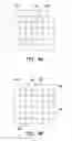
FIG. 1 is a perspective view of a semiconductor device according to an exemplary embodiment of the disclosure.
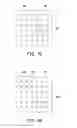
FIG. 2 is a diagram of a heating loop.
FIGS. 3A-3C respectively illustrates layouts of three heating loops.
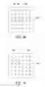
FIGS. 4A-4F are diagrams respectively illustrating six arrangements of first conductive elements and second conductive elements.
FIG. 5 is a perspective view of a semiconductor device according to another exemplary embodiment of the disclosure.
FIG. 6 is a partial cross-sectional view of a semiconductor device according to still another exemplary embodiment of the disclosure.
FIG. 7 is a flowchart illustrating an assembling method of a conductive device according to an exemplary embodiment of the disclosure.
FIGS. 8A-8C are cross-sectional views of a semiconductor device of FIG. 7 during an assembling process.
FIG. 9 is a flowchart illustrating an assembling method of a semiconductor device according to an exemplary embodiment of the disclosure.
DETAILED DESCRIPTION OF DISCLOSED EMBODIMENTS
The disclosure is directed to a semiconductor device, which can avoid damages caused by thermal stress and an electromigration effect.
The disclosure is directed to an assembling method of a semiconductor device, where the assembled semiconductor device can avoid damages caused by thermal stress and an electromigration effect.
The disclosure is directed to the semiconductor device and the assembling method thereof, the conductive elements with different composition ratios of the intermetallic compound can resist damages caused by the thermal stresses and the electromigration effect.
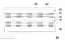
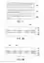
FIG. 1 is a perspective view of a semiconductor device according to an exemplary embodiment of the disclosure. Referring to FIG. 1, the semiconductor device 100 of the embodiment includes a chip 110, a carrier 120, a plurality of first conductive elements 130 and a plurality of second conductive elements 140. The chip 110 has a plurality of first pads 112. The carrier 120 has a plurality of second pads 122. Each first conductive element 130 disposed between one of the first pads 112 and one of the second pads 122. Each second conductive element 140 disposed between one of the first pads 112 and one of the second pads 122. A volume ratio of intermetallic compound (IMC) of the second conductive elements 140 is greater than a composition ratio of IMC of the first conductive elements 130. In the embodiment, the difference of the composition ratios of the IMC of the first conductive element 130 and the second conductive element 140 is formed when the semiconductor device 100 is manufactured, or is formed after the semiconductor device is sold.
For example, a material of the first conductive element 130 is tin-silver, and a material contact the first conductive element 130 is copper, the IMC in the second conductive element 140 is probably a tin-copper compound (for example, Cu3Sn or Cu6Sn5). Alternatively, the material of the first conductive element 130 is tin-silver-copper, and the material contact the first conductive element 130 is nickel, the IMC in the second conductive element 140 is probably a tin-nickel-copper compound (for example, (Cu,Ni)3Sn4 or (Cu,Ni)6Sn5). As the material of the first conductive element 130 is different to the material contact the first conductive element 130, a plurality of different IMCs can be simultaneously formed, for example. A percentage of the so-called volume ratio of the IMC is a total volume of the IMC relative to a total volume of the conductive element.
In the semiconductor device 100 of the embodiment, thermal expansion coefficients of the chip 110 and the carrier 120 are probably different, and during a temperature variation process that the temperature of the semiconductor device 100 is increased due to operation or is decreased due to non-operation, the first conductive elements 130 located between the chip 110 and the carrier 120 can bear relatively large thermal stress without being damaged due to relatively less volume ratio of the IMC and lower rigidity and hardness.
On the other hand, the second conductive elements 140 with relatively large volume ratio of the IMC have better resistance capability for the damage caused by an electromigration effect. Therefore, when the second conductive elements 140 serve as a conducting path of a large current, reliability of the semiconductor device 100 is improved.
The volume ratio of the IMC of the second conductive elements 140 even has a chance to be substantially 100%. Therefore, even the second conductive elements 140 serve as a main current input path, it can still greatly reduce possibility of the damage caused by the electromigration effect. Moreover, in the embodiment, the two types of conductive elements with different volume ratios of the IMC are taken as an example, though in other embodiments, more types of the conductive elements with different volume ratios of the IMC can also be simultaneously used.
The carrier 120 of the embodiment is, for example, a circuit substrate. However, in other embodiments, the carrier 120 can also be another chip. In other words, the technique of fabricating the conductive elements of different volume ratios of the IMC can be applied between the chip and the circuit substrate, and can also be applied between two chips or applied to other devices using the conductive elements as the electrical transmission path. Namely, the semiconductor device 100 of the embodiment can be formed by stacking a plurality of chips, and as long as the semiconductor device 100 includes the two types of conductive elements with different volume ratios of the IMC, it is considered to be within the protection scope of the disclosure.
The semiconductor device 100 of the embodiment further includes an underfill material 150 filled between the chip 110 and the carrier 120 and wrapping the first conductive elements 130 and the second conductive elements 140. The underfill material 150 is used to wrap the exposed parts of the first conductive elements 130 and the second conductive elements 140, and simultaneously slow the thermal stresses generated between the chip 110 and the carrier 120 due to the temperature variation, and further prevent external moisture from entering internal of the semiconductor device 100.
The carrier 120 of the embodiment further includes at least one heating loop 124. The heating loop 124 is electrically isolated to the second pads 122, namely, the heating loop 124 is not electrically connected to the second pads 122. Moreover, the heating loop 124 is adjacent to the second conductive elements 140. After a current is input to the heating loop 124, a temperature of the heating loop 124 is gradually increased due to the resistance thereof, and temperatures of the adjacent second conductive elements 140 are also increased. On the other hand, increasing of the temperatures of the first conductive elements 130 relatively far away from the heating loop 124 is less than that of the second conductive elements 140. Since the volume ratio of the IMC is increased as the temperature is increased, the first conductive elements 130 and the second conductive elements 140 with different volume ratios of the IMC are generated under a function of the heating loop 124. After the semiconductor device 100 is manufactured, the current of the heating loop 124 is cut off, and it is unnecessary to take out the heating circuit 124, which can be used to increase heat-dissipation efficiency of the working semiconductor device 100.
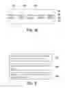
Moreover, a shape, a length and a resistance of the heating loop can be changed to increase the temperature of the second conductive elements heated by the heating loop, so as to effectively increase the volume ratio of the IMC of the second conductive elements. For example, a heating loop 200 of FIG. 2 can be designed to be battlements-like to increase a loop length to achieve higher resistance.
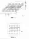
Moreover, a layout of the heating loop is determined according to positions of the second conductive elements required to generate relatively higher volume ratio of the IMC. For example, FIGS. 3A-3C respectively illustrates layouts of three heating loops 310, 320 and 330. In FIG. 3C, the number of the heating loops 330 is two, and the number of the heating loops 330 can be further increased according to an actual design requirement. Therefore, the heating loop of the exemplary embodiments of the disclosure can be designed into different geometric shapes to heat the first conductive elements and the second conductive elements.
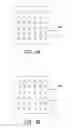
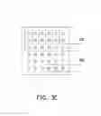
Relative positions of the first conductive elements and the second conductive elements can also be suitably adjusted, and a main consideration thereof is to configure the second conductive elements with higher volume ratio of the IMC at positions liable to have the electromigration effect due to a large current amount during utilization, and configure the first conductive elements with lower volume ratio of the IMC at positions bearing larger thermal stresses. FIGS. 4A-4F are diagrams respectively illustrating six arrangements of first conductive elements 410 and second conductive elements 420.
In FIG. 4A, the first conductive elements 410 are distributed at one side of the chip, and the second conductive elements 420 are distributed at most of the other regions. In order to achieve such distribution effect, a heating loop 432 can be predisposed in the region of the second conductive elements 420. In FIG. 4B, the first conductive elements 410 are distributed on the chip in an approximate T-shape, and the second conductive elements are disposed in other regions. Heating loops 434 can be predisposed in the region of the second conductive elements 420. In FIG. 4C, the first conductive elements 410 are disposed at periphery of the second conductive elements 420. A heating loop 436 can be predisposed in the region of the second conductive elements 420, and the current can be input along a direction perpendicular to a surface of the chip. In FIG. 4D, the first conductive elements 410 are disposed along a diagonal of the chip, and the second conductive bumps 420 are disposed at other regions in symmetric. A heating loop 438 can be predisposed in the region of the second conductive elements 420. In FIG. 4E, the second conductive elements 420 are disposed on the chip in a cross shape, and the first conductive elements 410 are disposed at other regions. A heating loop 442 can be predisposed in the region of the second conductive elements 420. In FIG. 4F, the second conductive elements 420 are disposed on the chip in an L-shape, and the first conductive elements 410 are disposed at other regions. A heating loop 444 can be predisposed in the region of the second conductive elements 420.
FIG. 5 is a perspective view of a semiconductor device according to another embodiment of the disclosure. Referring to FIG. 5, the semiconductor device 500 of the embodiment is similar to the semiconductor device 100 of FIG. 1, and a difference there between is that a carrier 520 of the embodiment does not include the heating loop, while a chip 510 has at least one heating loop 514. The heating loop 514 is isolated to the first pads 512, and is located adjacent to the second conductive elements 140. Namely, utilization methods, functions and possible variations of the heating loop 514 are the same to that of the heating loop 124 of FIG. 1.
FIG. 6 is a partial cross-sectional view of a semiconductor device according to still another embodiment of the disclosure. Referring to FIG. 6, the semiconductor device 600 of the embodiment is similar to the semiconductor device 100 of FIG. 1, and a difference there between is that the semiconductor device 600 of the embodiment further includes a chip 610, a plurality of third conductive elements 620 and a plurality of fourth conductive elements 630. The chip 610 has a plurality of third pads 612. The chip 110 disposed between the chip 610 and the carrier 120, and the chip 110 further has a plurality of fourth pads 114. Each third conductive element 620 disposed between one of the third pads 612 and one of the fourth pads 114. Each fourth conductive element 630 disposed between one of the third pads 612 and one of the fourth pads 114. A volume ratio of intermetallic compound of the third conductive elements 620 is greater than a volume ratio of intermetallic compound of the fourth conductive elements 630. Namely, the technique of fabricating the conductive elements of different volume ratios of the IMC can also be applied to the chip-stacked semiconductor device 600 to improve reliability of the chip-stacked semiconductor device 600.
FIG. 7 is a flowchart illustrating an assembling method of a conductive device according to an embodiment of the disclosure, and FIGS. 8A-8C are cross-sectional views of the semiconductor device of FIG. 7 during the assembling process. Referring to FIG. 7 and FIG. 8A, according to the assembling method of the semiconductor device of the embodiment, in step S110, a plurality of first pads 812 of a chip 810 is electrically connected to a plurality of second pads 822 of a carrier 820 through a plurality of first conductive elements 830. Now, all of the conductive elements between the first pads 812 and the second pads 822 are the first conductive elements 830, and compositions of all of the first conducive elements 830 are substantially the same without considering a fabrication process difference. The first conductive element 830 can be formed by a bump (not shown) on the first pad 812, a bump (not shown) on the second pad 822 and a solder between the two bumps. Materials of the two bumps can be tin-lead alloy, gold or other conductors. Moreover, under bump metallurgy (UBM) can be formed between the first pads 812 and the bumps, and the UBM can also be formed between the second pads 822 and the bumps. In addition, the first conductive element 830 can also be only formed by a bump (not shown) on the first pad 812 and a bump (not shown) on the second pad 822, and the two bumps are bonded through laser or other methods. Those skilled in the art should understand that methods of forming the first conductive elements 830 are diversified, which are not described in detail herein.
Then, referring to FIG. 7 and FIG. 8B, in step S120, a part of the first conductive elements 830 is heated to form a plurality of second conductive elements 840, and a volume ratio of IMC of the second conductive elements 840 is greater than a volume ratio of IMC of the first conductive elements 830. In detail, the volume ratio of the IMC of the heated first conductive elements 830 is increased, and the first conductive elements 830 with the increased volume ratio of the IMC are referred to as the second conductive elements 840, so as to form to two types of conductive elements with different volume ratios of the IMC. Methods for heating the first conductive elements 830 to form the second conductive elements 840 are plural, and one of the methods is to heat the first conductive elements 830 by using the heating loop 124 of the carrier 120 of FIG. 1 or the heating loop 514 of the chip 519 of FIG. 5. According to experiments, the method of heating the first conductive elements by applying power to the heating loop may even form the second conductive elements with the volume ratio of the IMC of 100%.
Referring to FIG. 7 and FIG. 8C, after the second conductive elements 840 are formed, in step S130, an underfill material 850 can be selectively filled between the chip 810 and the carrier 820. The underfill material 850 is the same to the underfill material 150 of FIG. 1.
FIG. 9 is a flowchart illustrating an assembling method of a semiconductor device according to an embodiment of the disclosure. Referring to FIG. 9, the assembling method of the semiconductor device of the embodiment is similar to that of the embodiment of FIG. 7, and a difference there between is that a step S140 of filling the underfill material is performed after the step S110 of electrically connecting the first pads to the second pads and before the step S120 of forming the second conductive elements.
In summary, in the semiconductor device and the assembling method thereof, two types of the conductive elements with different volume ratios of the IMC are formed. The conductive elements with smaller volume ratio of the IMC may have better resistance capability for the thermal stresses, and the conductive elements with larger volume ratio of the IMC have better resistance capability for the electromigration effect. Therefore, the semiconductor device and the assembling method thereof of the disclosure have better reliability.
It will be apparent to those skilled in the art that various modifications and variations can be made to the structure of the invention without departing from the scope or spirit of the invention. In view of the foregoing, it is intended that the invention cover modifications and variations of this invention provided they fall within the scope of the following claims and their equivalents.
Claims
What is claimed is:1. A semiconductor device, comprising:
a first chip, having a plurality of first pads;
a carrier, having a plurality of second pads, the second pads corresponding to the first pads;
a plurality of first conductive elements, respectively disposed between one of the first pads and one of the second pads; and
a plurality of second conductive elements, respectively disposed between one of the first pads and one of the second pads, wherein a volume ratio of intermetallic compound of the second conductive elements is greater than a volume ratio of intermetallic compound of the first conductive elements.
2. The semiconductor device as claimed in claim 1, wherein the volume ratio of intermetallic compound of the second conductive elements is substantially 100%.
3. The semiconductor device as claimed in claim 1, wherein the carrier is a circuit substrate or another chip.
4. The semiconductor device as claimed in claim 1, further comprising an underfill material filled between the first chip and the carrier and wrapping the first conductive elements and the second conductive elements.
5. The semiconductor device as claimed in claim 1, wherein the first chip further has at least one heating loop electrically isolated to the first pads and located adjacent to the second conductive elements.
6. The semiconductor device as claimed in claim 5, wherein the heating loop is battlement like.
7. The semiconductor device as claimed in claim 1, wherein the carrier further has at least one heating loop electrically isolated to the second pads and located adjacent to the second conductive elements.
8. The semiconductor device as claimed in claim 7, wherein the heating loop is battlement like.
9. The semiconductor device as claimed in claim 1, further comprising:
a second chip, having a plurality of third pads, wherein the first chip is located between the second chip and the carrier, and the first chip further has a plurality of fourth pads;
a plurality of third conductive elements, respectively disposed between one of the third pads and one of the fourth pads; and
a plurality of fourth conductive elements, respectively disposed between one of the third pads and one of the fourth pads, wherein a volume ratio of intermetallic compound of the third conductive elements is greater than a volume ratio of intermetallic compound of the fourth conductive elements.
10. An assembling method of a semiconductor device, comprising:
electrically connecting a plurality of first pads of a chip to a plurality of second pads of a carrier through a plurality of first conductive elements; and
heating a part of the first conductive elements to form a plurality of second conductive elements, wherein a volume ratio of intermetallic compound of the second conductive elements is greater than a volume ratio of intermetallic compound of the first conductive elements.
11. The assembling method of the semiconductor device as claimed in claim 10, wherein after the second conductive elements are formed, the method further comprises filling an underfill material between the chip and the carrier, wherein the underfill material wraps the first conductive elements and the second conductive elements.
12. The assembling method of the semiconductor device as claimed in claim 10, wherein after the step of electrically connecting the first pads to the second pads and before the step of forming the second conductive elements, the method further comprises filling an underfill material between the chip and the carrier, wherein the underfill material wraps the first conductive elements and the second conductive elements.
13. The assembling method of the semiconductor device as claimed in claim 10, wherein the step of forming the second conductive elements comprises powering at least a heating loop of the chip, wherein the heating loop is electrically isolated to the first pads and located adjacent to the second conductive elements.
14. The assembling method of the semiconductor device as claimed in claim 10, wherein the step of forming the second conductive elements comprises powering at least a heating loop of the carrier, wherein the heating loop is electrically isolated to the second pads and located adjacent to the second conductive elements.
Images & Drawings included:
Sources:
- United States Patent and Trademark Office - verify current appl. status at the USPTO↗
Similar patent applications:
- » 20120009734
Semiconductor device assembly and method thereof - » 20090294944
Semiconductor device assembly and method thereof - » 20090097804
Optical subassembly of optical semiconductor device module and assembly method thereof - » 20220028768
SEMICONDUCTOR DEVICE PACKAGES AND METHODS OF ASSEMBLING THEREOF - » 20100176508
Semiconductor device package and method of assembly thereof - » 20120015483
Semiconductor device package and method of assembly thereof - » 20240243095
SEMICONDUCTOR DEVICE ASSEMBLY, METHOD FOR MANUFACTURING SAME, AND APPLICATION THEREOF - » 20170309539
Control device and method for monitoring a function of a semiconductor component during the operation thereof and electrical assembly having a control device - » 20110241194
Stacked Semiconductor Device Package Assemblies with Reduced Wire Sweep and Manufacturing Methods Thereof - » 10211308
Semiconductor chip, chip-on-chip structure device, and assembling method thereof
Recent applications in this class:
- » 20250149490 2025-05-08
SEMICONDUCTOR PACKAGE - » 20250118694 2025-04-10
HONEYCOMB PATTERN FOR CONDUCTIVE FEATURES - » 20250112193 2025-04-03
SEMICONDUCTOR PACKAGE - » 20250096178 2025-03-20
MICROELECTRONIC PACKAGE WITH SOLDER ARRAY THERMAL INTERFACE MATERIAL (SA-TIM) - » 20250079379 2025-03-06
SEMICONDUCTOR DEVICE - » 20250006685 2025-01-02
SEMICONDUCTOR PACKAGES WITH MULTIPLE TYPES OF CONDUCTIVE COMPONENTS - » 20240421113 2024-12-19
UNIFORM CHIP GAPS VIA INJECTION-MOLDED SOLDER PILLARS - » 20240421112 2024-12-19
SEMICONDUCTOR ELEMENT AND SEMICONDUCTOR DEVICE - » 20240395755 2024-11-28
SEMICONDUCTOR PACKAGE - » 20240304583 2024-09-12
SEMICONDUCTOR DEVICE AND MANUFACTURING METHOD THEREOF
Recent applications for this Assignee:
- » 20250289330 2025-09-18
MOBILE VEHICLE CHARGING PROTECTION DEVICE FOR ELECTRICAL SAFETY IN LIVESTOCK HOUSES - » 20250287224 2025-09-11
COMMUNICATION DEVICE AND COMMUNICATION METHOD - » 20250286593 2025-09-11
COMMUNICATION DEVICE AND METHOD OF BEAM MANAGEMENT - » 20250284336 2025-09-11
SYSTEM AND METHOD FOR ADJUSTING IMAGE BASED ON PHYSIOLOGICAL INFORMATION AND POSTURE - » 20250281908 2025-09-11
ELECTROCATALYST COMPOSITION AND PREPARATION METHOD THEREOF - » 20250273403 2025-08-28
CAPACITOR AND ELECTRONIC DEVICE - » 20250271759 2025-08-28
POLYMER, POSITIVE PHOTORESIST COMPOSITION, AND METHOD FOR FORMING PATTERNED PHOTORESIST LAYER - » 20250265803 2025-08-21
MULTI-SENSOR COORDINATION METHOD, PROCESSING DEVICE, AND INFORMATION DISPLAY SYSTEM - » 20250263659 2025-08-21
METHOD AND KIT FOR PREPARING AN IMMUNE CELL DIFFERENTIATED FROM A STEM CELL - » 20250252547 2025-08-07
CORROSION POSITIONING SYSTEM, CORROSION INSPECTION VEHICLE AND CORROSION POSITIONING METHOD USING THE SAME