Au-based solder die attachment semiconductor device and method for manufacturing the same
US20160293522A1
2016-10-06
14/442,570
2013-11-13
✅ Patent granted
US 9,698,082 B2
2017-07-04
WO; PCT/JP2013/080695; 20131113
WO; WO2014/077282; 20140522
Nitin Parekh
Foley & Lardner LLP
2033-11-13
Abstract:
A semiconductor device according to the present invention, having an Au-based solder layer (3) sandwiched between a semiconductor element (1) and a Cu substrate (2) made mainly of Cu, in which the semiconductor device includes: a dense metal film (23) which is arranged between the Cu substrate (2) and the Au-based solder layer (3), and has fine slits (24) patterned to have a predetermined shape in a plan view; and fine structures (4) with dumbbell-like cross section, which have Cu and Au as main elements, and are each buried in the Cu substrate (2), the Au-based solder layer (3), and the fine slits (24) of the dense metal film (23).
Inventors:
- Satoshi TANIMOTO 15 🇯🇵 Yokohama-shi, Japan
- Shinji Sato 11 🇯🇵 Niiza-shi, Japan
- Hidekazu TANISAWA 1 🇯🇵 Niiza-shi, Japan
- Kohei MATSUI 1 🇯🇵 Kawasaki-shi, Japan
- Kohei MATSUI 6 🇯🇵 Hino, Japan
- Satoshi Tanimoto 14 🇯🇵 Yokohama, Japan
- Shinji Sato 9 🇯🇵 Niiza, Japan
- Hidekazu Tanisawa 1 🇯🇵 Niiza, Japan
Assignee:
- FUJI ELECTRIC CO., LTD. 2,338 🇯🇵 Kawasaki-shi, Japan
- FUJI ELECTRIC CO., LTD. 489 🇯🇵 Kawasaki-shi, Kanagawa, Japan
- Sanken Electric Co., Ltd. 419 🇯🇵 Niiza-shi, Japan
- NISSAN MOTOR CO., LTD. 2,119 🇯🇵 Yokohama-shi, Japan
- NISSAN MOTOR CO., LTD. 1,955 🇯🇵 Yokohama-shi, Kanagawa, Japan
- Sanken Electric Co., Ltd. 99 🇯🇵 Niiza-shi, Saitama, Japan
Applicant:
Interested in similar patents?
Get notified when new applications in this technology area are published.
Classification:
H01L23/49513 » CPC main
Details of semiconductor or other solid state devices; Arrangements for conducting electric current to or from the solid state body in operation, e.g. leads, terminal arrangements ; Selection of materials therefor consisting of soldered constructions; Lead-frames or other flat leads characterised by the die pad having bonding material between chip and die pad
H01L21/4853 » CPC further
Processes or apparatus adapted for the manufacture or treatment of semiconductor or solid state devices or of parts thereof; Manufacture or treatment of semiconductor devices or of parts thereof the devices having at least one potential-jump barrier or surface barrier, e.g. PN junction, depletion layer or carrier concentration layer; Manufacture or treatment of parts, e.g. containers, prior to assembly of the devices, using processes not provided for in a single one of the subgroups -; Conductive parts; Leads on or in insulating or insulated substrates, e.g. metallisation Connection or disconnection of other leads to or from a metallisation, e.g. pins, wires, bumps
H01L23/49548 » CPC further
Details of semiconductor or other solid state devices; Arrangements for conducting electric current to or from the solid state body in operation, e.g. leads, terminal arrangements ; Selection of materials therefor consisting of soldered constructions; Lead-frames or other flat leads; Geometry of the lead-frame Cross section geometry
H01L23/49562 » CPC further
Details of semiconductor or other solid state devices; Arrangements for conducting electric current to or from the solid state body in operation, e.g. leads, terminal arrangements ; Selection of materials therefor consisting of soldered constructions; Lead-frames or other flat leads; Geometry of the lead-frame for devices being provided for in
H01L23/49582 » CPC further
Details of semiconductor or other solid state devices; Arrangements for conducting electric current to or from the solid state body in operation, e.g. leads, terminal arrangements ; Selection of materials therefor consisting of soldered constructions; Lead-frames or other flat leads characterised by the materials of the lead frames or layers thereon Metallic layers on lead frames
H01L23/3735 » CPC further
Details of semiconductor or other solid state devices; Arrangements for cooling, heating, ventilating or temperature compensation ; Temperature sensing arrangements; Selection of materials, or shaping, to facilitate cooling or heating, e.g. heatsinks; Cooling facilitated by selection of materials for the device or materials for thermal expansion adaptation, e.g. carbon Laminates or multilayers, e.g. direct bond copper ceramic substrates
H01L24/29 » CPC further
Arrangements for connecting or disconnecting semiconductor or solid-state bodies; Methods or apparatus related thereto; Means for bonding being attached to, or being formed on, the surface to be connected, e.g. chip-to-package, die-attach, "first-level" interconnects; Manufacturing methods related thereto; Layer connectors, e.g. plate connectors, solder or adhesive layers; Manufacturing methods related thereto; Structure, shape, material or disposition of the layer connectors prior to the connecting process of an individual layer connector
H01L24/32 » CPC further
Arrangements for connecting or disconnecting semiconductor or solid-state bodies; Methods or apparatus related thereto; Means for bonding being attached to, or being formed on, the surface to be connected, e.g. chip-to-package, die-attach, "first-level" interconnects; Manufacturing methods related thereto; Layer connectors, e.g. plate connectors, solder or adhesive layers; Manufacturing methods related thereto; Structure, shape, material or disposition of the layer connectors after the connecting process of an individual layer connector
H01L24/83 » CPC further
Arrangements for connecting or disconnecting semiconductor or solid-state bodies; Methods or apparatus related thereto; Methods for connecting semiconductor or other solid state bodies using means for bonding being attached to, or being formed on, the surface to be connected using a layer connector
H01L23/4827 » CPC further
Details of semiconductor or other solid state devices; Arrangements for conducting electric current to or from the solid state body in operation, e.g. leads, terminal arrangements ; Selection of materials therefor consisting of lead-in layers inseparably applied to the semiconductor body Materials
H01L24/03 » CPC further
Arrangements for connecting or disconnecting semiconductor or solid-state bodies; Methods or apparatus related thereto; Means for bonding being attached to, or being formed on, the surface to be connected, e.g. chip-to-package, die-attach, "first-level" interconnects; Manufacturing methods related thereto; Bonding areas ; Manufacturing methods related thereto Manufacturing methods
H01L24/05 » CPC further
Arrangements for connecting or disconnecting semiconductor or solid-state bodies; Methods or apparatus related thereto; Means for bonding being attached to, or being formed on, the surface to be connected, e.g. chip-to-package, die-attach, "first-level" interconnects; Manufacturing methods related thereto; Bonding areas ; Manufacturing methods related thereto; Structure, shape, material or disposition of the bonding areas prior to the connecting process of an individual bonding area
H01L24/75 » CPC further
Arrangements for connecting or disconnecting semiconductor or solid-state bodies; Methods or apparatus related thereto; Apparatus for manufacturing arrangements for connecting or disconnecting semiconductor or solid-state bodies Apparatus for connecting with bump connectors or layer connectors
H01L2224/0345 » CPC further
Indexing scheme for arrangements for connecting or disconnecting semiconductor or solid-state bodies and methods related thereto as covered by; Means for bonding being attached to, or being formed on, the surface to be connected, e.g. chip-to-package, die-attach, "first-level" interconnects; Manufacturing methods related thereto; Bonding areas; Manufacturing methods related thereto; Manufacturing methods by blanket deposition of the material of the bonding area in gaseous form Physical vapour deposition [PVD], e.g. evaporation, or sputtering
H01L2224/04026 » CPC further
Indexing scheme for arrangements for connecting or disconnecting semiconductor or solid-state bodies and methods related thereto as covered by; Means for bonding being attached to, or being formed on, the surface to be connected, e.g. chip-to-package, die-attach, "first-level" interconnects; Manufacturing methods related thereto; Bonding areas; Manufacturing methods related thereto; Structure, shape, material or disposition of the bonding areas prior to the connecting process Bonding areas specifically adapted for layer connectors
H01L2224/2732 » CPC further
Indexing scheme for arrangements for connecting or disconnecting semiconductor or solid-state bodies and methods related thereto as covered by; Means for bonding being attached to, or being formed on, the surface to be connected, e.g. chip-to-package, die-attach, "first-level" interconnects; Manufacturing methods related thereto; Layer connectors, e.g. plate connectors, solder or adhesive layers; Manufacturing methods related thereto; Manufacturing methods by local deposition of the material of the layer connector in liquid form Screen printing, i.e. using a stencil
H01L2224/3207 » CPC further
Indexing scheme for arrangements for connecting or disconnecting semiconductor or solid-state bodies and methods related thereto as covered by; Means for bonding being attached to, or being formed on, the surface to be connected, e.g. chip-to-package, die-attach, "first-level" interconnects; Manufacturing methods related thereto; Layer connectors, e.g. plate connectors, solder or adhesive layers; Manufacturing methods related thereto; Structure, shape, material or disposition of the layer connectors after the connecting process of an individual layer connector; Shape of bonding interfaces, e.g. interlocking features
H01L2224/32505 » CPC further
Indexing scheme for arrangements for connecting or disconnecting semiconductor or solid-state bodies and methods related thereto as covered by; Means for bonding being attached to, or being formed on, the surface to be connected, e.g. chip-to-package, die-attach, "first-level" interconnects; Manufacturing methods related thereto; Layer connectors, e.g. plate connectors, solder or adhesive layers; Manufacturing methods related thereto; Structure, shape, material or disposition of the layer connectors after the connecting process of an individual layer connector; Material outside the bonding interface, e.g. in the bulk of the layer connector
H01L2224/7501 » CPC further
Indexing scheme for arrangements for connecting or disconnecting semiconductor or solid-state bodies and methods related thereto as covered by; Apparatus for manufacturing arrangements for connecting or disconnecting semiconductor or solid-state bodies and for methods related thereto; Apparatus for connecting with bump connectors or layer connectors Means for cleaning, e.g. brushes, for hydro blasting, for ultrasonic cleaning, for dry ice blasting, using gas-flow, by etching, by applying flux or plasma
H01L2224/75102 » CPC further
Indexing scheme for arrangements for connecting or disconnecting semiconductor or solid-state bodies and methods related thereto as covered by; Apparatus for manufacturing arrangements for connecting or disconnecting semiconductor or solid-state bodies and for methods related thereto; Apparatus for connecting with bump connectors or layer connectors; Means for controlling the bonding environment, e.g. valves, vacuum pumps; Chamber Vacuum chamber
H01L2224/75251 » CPC further
Indexing scheme for arrangements for connecting or disconnecting semiconductor or solid-state bodies and methods related thereto as covered by; Apparatus for manufacturing arrangements for connecting or disconnecting semiconductor or solid-state bodies and for methods related thereto; Apparatus for connecting with bump connectors or layer connectors; Means for applying energy, e.g. heating means in the lower part of the bonding apparatus, e.g. in the apparatus chuck
H01L2224/75756 » CPC further
Indexing scheme for arrangements for connecting or disconnecting semiconductor or solid-state bodies and methods related thereto as covered by; Apparatus for manufacturing arrangements for connecting or disconnecting semiconductor or solid-state bodies and for methods related thereto; Apparatus for connecting with bump connectors or layer connectors; Means for aligning; Guiding structures in the upper part of the bonding apparatus, e.g. in the bonding head
H01L2224/8309 » CPC further
Indexing scheme for arrangements for connecting or disconnecting semiconductor or solid-state bodies and methods related thereto as covered by; Methods for connecting semiconductor or other solid state bodies using means for bonding being attached to, or being formed on, the surface to be connected using a layer connector; Bonding environment Vacuum
H01L2224/83011 » CPC further
Indexing scheme for arrangements for connecting or disconnecting semiconductor or solid-state bodies and methods related thereto as covered by; Methods for connecting semiconductor or other solid state bodies using means for bonding being attached to, or being formed on, the surface to be connected using a layer connector; Pre-treatment of the layer connector or the bonding area; Cleaning the layer connector, e.g. oxide removal step, desmearing Chemical cleaning, e.g. etching, flux
H01L2224/8321 » CPC further
Indexing scheme for arrangements for connecting or disconnecting semiconductor or solid-state bodies and methods related thereto as covered by; Methods for connecting semiconductor or other solid state bodies using means for bonding being attached to, or being formed on, the surface to be connected using a layer connector; Applying energy for connecting using a reflow oven
H01L2224/83022 » CPC further
Indexing scheme for arrangements for connecting or disconnecting semiconductor or solid-state bodies and methods related thereto as covered by; Methods for connecting semiconductor or other solid state bodies using means for bonding being attached to, or being formed on, the surface to be connected using a layer connector; Pre-treatment of the layer connector or the bonding area Cleaning the bonding area, e.g. oxide removal step, desmearing
H01L2224/83048 » CPC further
Indexing scheme for arrangements for connecting or disconnecting semiconductor or solid-state bodies and methods related thereto as covered by; Methods for connecting semiconductor or other solid state bodies using means for bonding being attached to, or being formed on, the surface to be connected using a layer connector; Pre-treatment of the layer connector or the bonding area Thermal treatments, e.g. annealing, controlled pre-heating or pre-cooling
H01L2224/83075 » CPC further
Indexing scheme for arrangements for connecting or disconnecting semiconductor or solid-state bodies and methods related thereto as covered by; Methods for connecting semiconductor or other solid state bodies using means for bonding being attached to, or being formed on, the surface to be connected using a layer connector; Bonding environment; Composition of the atmosphere being inert
H01L2224/83101 » CPC further
Indexing scheme for arrangements for connecting or disconnecting semiconductor or solid-state bodies and methods related thereto as covered by; Methods for connecting semiconductor or other solid state bodies using means for bonding being attached to, or being formed on, the surface to be connected using a layer connector the layer connector being supplied to the parts to be connected in the bonding apparatus as prepeg comprising a layer connector, e.g. provided in an insulating plate member
H01L2224/83385 » CPC further
Indexing scheme for arrangements for connecting or disconnecting semiconductor or solid-state bodies and methods related thereto as covered by; Methods for connecting semiconductor or other solid state bodies using means for bonding being attached to, or being formed on, the surface to be connected using a layer connector; Bonding interfaces outside the semiconductor or solid-state body Shape, e.g. interlocking features
H01L2224/83815 » CPC further
Indexing scheme for arrangements for connecting or disconnecting semiconductor or solid-state bodies and methods related thereto as covered by; Methods for connecting semiconductor or other solid state bodies using means for bonding being attached to, or being formed on, the surface to be connected using a layer connector; Bonding techniques; Soldering or alloying Reflow soldering
H01L2924/01322 » CPC further
Indexing scheme for arrangements or methods for connecting or disconnecting semiconductor or solid-state bodies as covered by; Alloys; Binary Alloys Eutectic Alloys, i.e. obtained by a liquid transforming into two solid phases
H01L2924/12042 » CPC further
Indexing scheme for arrangements or methods for connecting or disconnecting semiconductor or solid-state bodies as covered by; Details of semiconductor or other solid state devices to be connected; Device type; Passive devices, e.g. 2 terminal devices; Optical Diode LASER
H01L2924/15747 » CPC further
Indexing scheme for arrangements or methods for connecting or disconnecting semiconductor or solid-state bodies as covered by; Details of package parts other than the semiconductor or other solid state devices to be connected; Die mounting substrate; Material with a principal constituent of the material being a metal or a metalloid, e.g. boron [B], silicon [Si], germanium [Ge], arsenic [As], antimony [Sb], tellurium [Te] and polonium [Po], and alloys thereof the principal constituent melting at a temperature of greater than or equal to 950 C and less than 1550 C Copper [Cu] as principal constituent
H01L2924/15787 » CPC further
Indexing scheme for arrangements or methods for connecting or disconnecting semiconductor or solid-state bodies as covered by; Details of package parts other than the semiconductor or other solid state devices to be connected; Die mounting substrate; Material with a principal constituent of the material being a non metallic, non metalloid inorganic material Ceramics, e.g. crystalline carbides, nitrides or oxides
H01L2924/35121 » CPC further
Indexing scheme for arrangements or methods for connecting or disconnecting semiconductor or solid-state bodies as covered by; Technical effects; Mechanical effects; Thermal stress; Cracking Peeling or delaminating
H01L2924/3651 » CPC further
Indexing scheme for arrangements or methods for connecting or disconnecting semiconductor or solid-state bodies as covered by; Technical effects; Material effects; Metallurgical effects Formation of intermetallics
H01L23/48 IPC
Details of semiconductor or other solid state devices Arrangements for conducting electric current to or from the solid state body in operation, e.g. leads, terminal arrangements ; Selection of materials therefor
H01L23/495 IPC
Details of semiconductor or other solid state devices; Arrangements for conducting electric current to or from the solid state body in operation, e.g. leads, terminal arrangements ; Selection of materials therefor consisting of soldered constructions Lead-frames or other flat leads
H01L23/488 » CPC further
Details of semiconductor or other solid state devices; Arrangements for conducting electric current to or from the solid state body in operation, e.g. leads, terminal arrangements ; Selection of materials therefor consisting of soldered constructions
H01L23/492 » CPC further
Details of semiconductor or other solid state devices; Arrangements for conducting electric current to or from the solid state body in operation, e.g. leads, terminal arrangements ; Selection of materials therefor consisting of soldered constructions Bases or plates or solder therefor
H01L23/373 IPC
Details of semiconductor or other solid state devices; Arrangements for cooling, heating, ventilating or temperature compensation ; Temperature sensing arrangements; Selection of materials, or shaping, to facilitate cooling or heating, e.g. heatsinks Cooling facilitated by selection of materials for the device or materials for thermal expansion adaptation, e.g. carbon
H01L21/48 IPC
Processes or apparatus adapted for the manufacture or treatment of semiconductor or solid state devices or of parts thereof; Manufacture or treatment of semiconductor devices or of parts thereof the devices having at least one potential-jump barrier or surface barrier, e.g. PN junction, depletion layer or carrier concentration layer Manufacture or treatment of parts, e.g. containers, prior to assembly of the devices, using processes not provided for in a single one of the subgroups -
H01L23/482 IPC
Details of semiconductor or other solid state devices; Arrangements for conducting electric current to or from the solid state body in operation, e.g. leads, terminal arrangements ; Selection of materials therefor consisting of lead-in layers inseparably applied to the semiconductor body
H01L23/00 IPC
Details of semiconductor or other solid state devices
Description
TECHNICAL FIELD
The present invention relates to a semiconductor device having a Cu substrate and a semiconductor element joined with an Au-based solder, and a method for manufacturing the same.
BACKGROUND ART
There has been developed a power semiconductor device using a wide band gap semiconductor made of silicon carbide (SiC), gallium nitride (GaN), diamond (C) or the like. Such a power semiconductor device, although operated at a high semiconductor joint temperature (Tj), has an on-resistance lower than that of a conventional power semiconductor device using silicon (Si) or gallium arsenic (GaAs), and thus is capable of fast switching. Therefore, reduction in chip size of the semiconductor device as well as reduction in size of a passive component and a cooler included in a system can be achieved. Thus, it is expected that a small, light and inexpensive power electronics system can be realized.
As a matter of course, high heat resistance is demanded for a joint portion, i.e., die attachment between a semiconductor element chip and a metal substrate, which are included in such a power semiconductor device operated at such a high semiconductor joint temperature (Tj). From the viewpoint of electric conductivity, thermal conductivity and price, a plate material mainly made of copper (Cu) is generally used as the metal substrate. Such a plate material is mostly used in a state of being attached to a ceramic insulating substrate. Hereinafter, substrates including the one having the plate material attached to the ceramic insulating substrate are simply referred to as a “Cu substrate”.
Meanwhile, high melting point Au-based solder is widely used as a joint material (see Non Patent Literatures 1 to 3). The Au-based solder described here includes eutectic AuGe solder (melting point of 356° C.), eutectic AuSi solder (melting point of 363° C.), eutectic AuSn solder (melting point of 280° C.), and the like.
CITATION LIST
Non Patent Literature
Non Patent Literature 1: P. Alexandrov, W. Wright, M. Pan, M. Weiner, L. Jiao, J. H. Zhao, Solid-State Electron., 47 (2003) p. 263.
Non Patent Literature 2: R. W. Johnson and L. Williams, Mater. Sci. Forum 483-485 (2005) p. 785
Non Patent Literature 3: S. Tanimoto, K. Matsui, Y. Murakami, H. Yamaguchi, and H. Okumura, Proceedings of IMAPS HiTEC 2010 (May 11-13, 2010, Albuquerque, N.Mex., USA), pp. 32-39.
SUMMARY OF INVENTION
The Au-based solder die attachment of the conventional semiconductor device has a configuration in which the Au-based solder layer joined with a semiconductor element (SiC) chip is separated from the Cu substrate by applying a dense plating of Ni or the like, that functions as a barrier metal, to the Cu substrate. However, when such a semiconductor device is used over a long period of time at high temperature, joint strength of a solder joint layer is lowered with time. This leads to a problem that the semiconductor chip eventually comes off around the plating layer. This deterioration phenomenon occurs more significantly and in a shorter period of time at higher temperature.
In Non Patent Literature 3 described above, for example, when a die attachment having an SiC chip joined with AuGe solder on an Ni plating Cu plate is left in an atmosphere of 300° C., the joint strength is reported to be lowered to near the lower limit specified in IEC60749-19 standard after about 3000 hours.
The present invention has been made to solve such conventional problems. It is an object of the present invention to provide an Au-based solder die attachment semiconductor device capable of extending a peel-off mode life by delaying deterioration of joint strength due to heating of the semiconductor device, and to provide a method for manufacturing the same.
In order to achieve the above object, the invention of the present application includes a dense metal film provided between a Cu substrate and an Au-based solder layer, the dense metal film having fine slits pattern to have a predetermined shape in a plan view. Also, fine structures with dumbbell-like cross section, which have Cu and Au as main elements, are each buried in the Cu substrate, the Au-based solder layer, and the fine slits in the dense metal film.
BRIEF DESCRIPTION OF DRAWINGS
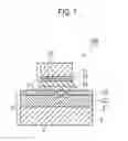
FIG. 1 is a cross-sectional view showing a main part of a semiconductor device according to an embodiment of the present invention.
FIG. 2 is a cross-sectional view showing a method for manufacturing the semiconductor device shown in FIG. 1.
FIG. 3 is a photograph of a fine structure with dumbbell-like cross section, which is taken by a scanning electron microscope, in the cross-section of the semiconductor device manufactured by the method for manufacturing a semiconductor device according to the present invention.
FIG. 4 is an explanatory diagram showing, in comparison with a conventional example, joint strength when the semiconductor device according to the embodiment is left for 3000 hours at 300° C.
FIG. 5 is an explanatory diagram showing examples of a fine silt shape of a dense metal film used in the semiconductor device according to the present invention.
DESCRIPTION OF EMBODIMENTS
With reference to the drawings, an embodiment of the present invention is described below. FIG. 1 is a cross-sectional view showing a configuration of a semiconductor device according to one embodiment of the present invention. Note that, in cross-sectional views used to explain the structure of this embodiment, dimensions in a thickness direction (vertical direction in the drawings) are exaggeratingly described to facilitate the understanding thereof.
Moreover, the following description is given of a case, as an example, where an SiC power element is used as a semiconductor element 1, eutectic AuGe solder is used as an Au-based solder layer 3, and an SiN ceramic substrate having metal Cu plates, mainly made of Cu, attached on both surfaces thereof is used as a Cu substrate 2.
However, this is just an example, and another wide band gap semiconductor element, such as a GaN element, a diamond element and a ZnO element, or an Si semiconductor element (SOI element or sensor element) for high-temperature application can be equally applied as the semiconductor element 1.
Also, Au-based solder used as the Au-based solder layer 3 is mainly made of Au, and typical examples thereof include eutectic AuGe solder, eutectic AuSi solder, eutectic AuSn solder, and the like. Moreover, a mixture of the solders described above or one obtained by adding another element to the eutectic solders may also be used. Furthermore, the solder does not necessarily have to have an eutectic composition but may have a hypereutectic or hypoeutectic composition having a liquidus temperature of approximately 420° C. or less.
Meanwhile, the Cu substrate 2 is not limited to the Cu substrate attached to the SiN ceramic substrate, but the Cu substrate attached to other types of ceramic substrate (such as alumina, aluminum nitride and beryllia) or a simple metal plate mainly made of Cu, such as a lead frame, may be used as the Cu substrate 2.
As shown in FIG. 1, a semiconductor device 100 according to this embodiment has a die attach structure in which the Cu substrate 2 and the semiconductor element 1 (semiconductor element chip) are joined with the Au-based solder layer 3. In other words, the semiconductor device 100 according to this embodiment is an Au-based solder die attachment semiconductor device having a die attachment structure in which the Au-based solder layer 3 is sandwiched between the semiconductor element chip (semiconductor element 1) and the Cu substrate 2 mainly made of Cu.
The semiconductor element 1 is a silicon carbide (SiC) power semiconductor element, and an ohmic contact 11 is formed on a back surface (lower surface in FIG. 1) thereof. The surface of (below in FIG. 1) the ohmic contact 11 is covered with a mounting electrode 12 for the purpose of improvement in solder wettability, prevention of solder intrusion, improvement in adhesion, and the like. As the mounting electrode 12, a Ti/Ni/Ag laminated deposited film (layer structure having Ti in contact with the ohmic contact 11 and Ag on the top), can be used, for example.
The Cu substrate 2 has a structure in which a metal Cu plate 22 mainly made of Cu is attached to at least one surface of the SiN ceramic substrate 21 by brazing or the like. On the surface of the metal Cu plate 22, a dense metal film 23 having fine slits 24 is provided. The dense metal film 23 is a metal film made of an Ni film, a Co film, an NiCo mixed film (both of Ni and Co), an Ni/Co laminated film, or the like. The dense metal film 23 functions to ensure wettability of soldering and to prevent the Au-based solder layer 3 and the metal Cu plate 22 from coming into full contact with each other. Moreover, the dense metal film 23 has a thickness of less than 10 μm, and the easiest and cheapest way to form the dense metal film 23 is electroless plating. However, the dense metal film 23 may be formed by another film formation method such as sputtering and electron beam method. In this event, an Ni film or a Co film formed by electroless plating becomes an Ni—P film or a Co—P film having high concentrations of P (phosphorus).
The fine slits 24 in the dense metal film 23 are extended linearly at a predetermined angle in a direction perpendicular to the page space, and patterned to have a predetermined shape in a plan view (when the semiconductor device 100 shown in FIG. 1 is viewed from above). FIG. 5 is an explanatory diagram showing examples of the shape of the fine slits 24 when the dense metal film 23 is planarly viewed. FIG. 5(a) shows an example of a rectangular periodic pattern in which slits are formed into a rectangular shape. FIG. 5(b) shows an example of a hexagonal periodic pattern in which slits are formed into a hexagonal shape. FIG. 5(c) shows an example of an equally spaced parallel line pattern in which slits are formed on parallel lines. FIG. 5(d) shows an example of a houndstooth rectangular periodic pattern in which slits are formed into a houndstooth shape. FIG. 5(e) shows an example of a trigonal periodic pattern in which slits are formed into a triangular shape. In other words, the slits shown in FIGS. 5(a) to 5(e) are formed in a pattern in which the same shape is repeatedly formed when planarly viewed, i.e., in a two-dimensional periodic pattern.
Among those shown in FIGS. 5(a) to 5(e), it is more preferable to use the rectangular periodic pattern shown in FIG. 5(a) and the hexagonal periodic pattern shown in FIG. 5(b). Moreover, it is preferable that the width of the slit takes a value between a value equivalent to the thickness of a solder layer to be described later as the maximum value and the minimum value of 0.1 μm. It is more preferable that the width of the slit is within a range of 20 μm to 1 μm.
Moreover, in a perspective view of the semiconductor device 100 according to this embodiment from the upper surface side of the semiconductor element 1 toward the Cu substrate 2, a ratio of the cumulative area of the slits to the whole joint surface of the semiconductor chip, i.e., a ratio of the total orthogonal projection area of the fine slits 24 to the whole junction area of the semiconductor element 1 is preferably 0.1% to 10%, more preferably, 5% or less.
The Au-based solder layer 3 shown in FIG. 1 is a layer formed by including Cu in eutectic AuGe solder, for example. Cu included in the Au-based solder layer 3 is derived from the metal Cu plate 22 in the Cu substrate 2.
More specifically, the Au-based solder layer 3 includes Cu derived from the Cu substrate 2, as an active component.
Here, it is one of the distinctive structural characteristics of the present invention that the Au-based solder layer 3 includes Cu and that Cu is derived from the Cu substrate 2.
Furthermore, fine structures 4 with dumbbell-like cross section, which have Cu and Au as main elements, are formed so as to fill in the fine slits 24 formed in the dense metal film 23. More specifically, the fine structures 4 with dumbbell-like cross section, which have Cu and Au as main elements, are each buried in the Cu substrate 2, the Au-based solder layer 3 and the fine slits 24 in the dense metal film 23. The formation of such fine structures 4 with dumbbell-like cross section is another distinctive structural characteristic of the present invention. Here, the fine structures 4 with dumbbell-like cross section each refer to a region having the cross-section indicated by the dotted line in FIG. 1. The dumbbells of the fine structures 4 with dumbbell-like cross section are formed inside the Au-based solder layer 3 on the dense metal film 23 and inside the metal Cu plate 22 through the fine slits 24. Thus, the Au-based solder layer 3 and the Cu substrate 2 can be firmly connected, and the fine structures 4 with dumbbell-like cross section function as solder connection means for connecting the Cu substrate 2 and the Au-based solder layer 3. Moreover, as described later, Cu and Au as the main elements of the fine structures 4 with dumbbell-like cross section are derived from the Cu substrate 2 and the Au-based solder layer 3, respectively.
Next, steps of manufacturing the semiconductor device shown in FIG. 1 are described with reference to process drawings shown in FIGS. 2(a) to 2(c). First, as shown in FIG. 2(a), precursor materials A1, B2 and C3 are prepared. The precursor material A1 is the power semiconductor element 1 made of silicon carbide (SiC) shown in FIG. 1 described above. The structure of the mounting electrode 12 on the back surface of the silicon carbide (SiC) power semiconductor element 1 that is commercially available is virtually almost the same as the mounting electrode structure described above. Thus, there is no particular need for modifications to implement the present invention as long as such structures are used.
The precursor material B2 is the Cu substrate 2 shown in FIG. 1. The precursor material B2 is prepared through the following procedures. First, a commercially available Cu substrate 2 formed by attaching a metal Cu plate 22 on the surface of a ceramic substrate 21 by an active metal method or a direct joint method is prepared. Then, on the surface of the Cu substrate 2, a dense metal film (e.g., an Ni—P film having a thickness of 5 μm) 23 having fine slits 24 is formed by pattern electroless plating. The pattern plating described here is a method in which a photoresist is applied by photolithography only to portions corresponding to the fine slits 24 in the surface of the Cu substrate 2 and then plating is performed to grow Ni—P plating only in a Cu surface exposed portion without photoresist. As a result, the fine slits 24 are formed at designed positions. Then, the photoresist is removed with a solvent after the plating.
In this event, the fine slits 24 are formed to have a two-dimensional periodic pattern (predetermined pattern), as shown in FIGS. 5(a) to 5(e) described above, when planarly viewed.
As a method for forming the fine slits 24, etching, laser beam processing or other methods may be used other than the pattern plating. When etching or laser beam processing is adopted, etching or laser beam processing is performed after an Ni—P film is grown by plating on the entire surface of the metal Cu plate 22. In this event, a resist pattern is formed before the etching process.
At the bottoms of the fine slits 24, relatively easily oxidizable Cu (metal Cu plate 22) is exposed as shown in FIG. 2(b). In such a case as long-term storage, CuO is formed on the surface of the exposed metal Cu plate 22, which deteriorates wettability of the Au-based solder. To avoid such a problem, a thin Ni—P plating film (having a thickness of less than 0.2 μm) may be formed by electroless plating on the entire surface of the conductor part immediately after the dense metal film 23 is formed by pattern plating. Thus, the surface of the metal Cu plate 22, which serves as the bottoms of the fine slits 24, is covered with a thin Ni plating film (not shown in FIG. 2). In other words, it is preferable, in preventing the formation of CuO, that a process of covering the dense metal film 23 with a plating film having a thickness of less than 0.2 μm on the entire surface of the Cu substrate 2 is added to the final step of the processing of forming the dense metal film 23 having the fine slits 24 on the Cu substrate surface.
Next, although not essential, a thin Au film or Ag film may be applied by flushing plating onto the dense metal film 23. Accordingly, in a subsequent reflow process, the solder wettability is further improved, and thus the yield can be improved.
The precursor material C3 shown in FIG. 2(a) is an Au-based solder material 3a mainly made of Au, and is typically eutectic AuGe solder, eutectic AuSi solder, eutectic AuSn solder, or the like. Alternatively, a mixture of these solders may be used. Furthermore, the solder does not necessarily have to have an eutectic composition but may have a hypereutectic or hypoeutectic composition having a liquidus temperature of approximately 420° C. or less. Moreover, the precursor material C3 may include a third element as impurities to improve modification, and may be prepared as a preform (chip-shaped solid) or paste.
One of the points to be noted is that the Au-based solder material 3a used as the precursor material C3 and the Au-based solder layer 3 (see FIG. 1) in the completed semiconductor device 100 do not have the same constituent elements. Cu, which is not included in the Au-based solder material 3a as the precursor material C3, is included as an active component in the Au-based solder layer 3.
Once the preparation of the precursor materials A1, B2 and C3 is completed, organic cleaning is performed using a solvent such as acetone and isopropyl alcohol to remove contaminants adhering to the surface of each of the precursor materials A1, B2 and C3.
Subsequently, the precursor materials A1, B2 and C3 are placed in a decompression reflow device. It is assumed that the decompression reflow device has exhaust capability to reduce the pressure to about 5 millibar and has specifications to introduce inert gas (nitrogen or argon gas) having a purity of 99.99% or more.
Instead of the decompression reflow device, an atmospheric reflow device is capable of executing reflow in a reductive atmosphere or low dew point atmosphere.
Thereafter, the precursor material B2 (the Cu substrate 2) is placed on a reflow stage of the decompression reflow device, the precursor material C3 (the Au-based solder material 3a) is placed (applied when it is a paste) in a portion to be joined on the precursor material B2, and the precursor material A1 (the semiconductor element 1) is further placed thereon, as shown in FIG. 2(a). More specifically, an overlay process is performed to sequentially overlay the Cu substrate 2 coated with the dense metal film 23 having the fine slits 24, the Au-based solder material 3a having a liquidus temperature of 420° C. or less, and the semiconductor element chip (semiconductor element 1) on a heating stage (reflow stage). Note that the illustration of the reflow stage is omitted in FIG. 2.
Here, in order to prevent a positional shift of the semiconductor element 1 during a reflow process by accurately placing the precursor material C3 and the precursor material A1 in the portion to be joined on the precursor material B2, it is desirable to use a template carbon jig.
Note that, although not a requirement of the present invention, gentle pressure may be applied lo the semiconductor element 1 during the reflow process, particularly, during solder melting, in order to reduce voids to be generated in the Au-based solder layer 3 shown in FIG. I. A required load is 0.1 g/cm2 or more, preferably, 0.3 g/cm2 or more. For the semiconductor element 1 with an area of 4 mm2, for example, a load of 0.4 g or more, preferably, 1.2 g or more may be used.
Once the above preparation is completed, the reflow process is executed. The reflow process is described in detail below. First, a sample chamber in the decompression reflow device is evacuated. When the pressure inside the sample chamber is reduced to 5 millibar or less, inert gas is introduced. This operation is performed several times to replace the air inside the sample chamber with the inert gas. Thus, the sample chamber is filled with the inert gas.
Then, the reflow stage or the entire sample chamber is heated to raise the temperature of the precursor materials A1, B2 and C3 to approximately 200° C., and the temperature is maintained for about 2 minutes. In this event, inert gas containing formic acid vapor is introduced to facilitate removal of organic contaminants.
Next, the introduction of the inert gas is stopped, and the evacuation is resumed to reduce the pressure in the sample chamber to 5 millibar or less. Moreover, the reflow stage (or the entire sample chamber) is further heated to raise the temperature of the precursor materials A1, B2 and C3 to the liquidus temperature or more of the Au-based solder material 3a, and the temperature is maintained. As the time for maintaining the temperature, 5 minutes is sufficient at the longest. When the precursor material C3 (Au-based solder material 3a) is eutectic AuGe solder, for example, typical reflow conditions include the temperature of 410° C. and 1 minute. When the temperature of the precursor material C3 exceeds the liquidus temperature, the precursor material C3 melts to wet the surface of the dense metal film 23 and the back surface of the semiconductor element 1.
In this event, as shown in FIG. 2(b), a melt (Au-based solder melt 3b) of the precursor material C3 flows into the fine slits 24 by capillary action or the like and fills in the fine slits 24 in the dense metal film 23 (Ni—P plating film). Then, the Au-based solder melt 3b very actively exchanges atoms of Au and Cu on the interface between the melt and the solid while melting the surface of the metal Cu plate 22 at the bottoms of the fine slits 24. Cu emitted from the metal Cu plate 22 melts into the layer of the Au-based solder melt 3b, easily moves and rapidly spreads across the entire layer of the Au-based solder melt 3b. As a result, the composition of a layer of an Au-based solder melt 3′ is changed from Au+Ge to Au+Cu+Ge.
Meanwhile, as shown in FIG. 2(c), Au atoms emitted from the layer of the Au-based solder melt 3′ containing Cu into the metal Cu plate 22 approximately isotropically spread in Cu as the solid, and modify the composition of the spread region into an Au+Cu alloy 4′. Thus, a precursor structure of the fine structures 4 with dumbbell-like cross section is formed. More specifically, the main elements Cu and Au in the fine structures 4 with dumbbell-like cross section are derived from the Cu substrate 2 and the Au-based solder layer 3, respectively. Note that, at this point, the Au-based solder layer 3 is in the liquid phase, and thus the term “precursor structure” is used.
As described above, a heating process is performed, in which the Cu substrate 2, the Au-based solder material 3 a and the semiconductor element chip (semiconductor element 1), which are overlaid on the heating stage (reflow stage), are heated to raise the temperature thereof, and then the Au-based solder material 3a is melted to form a melt layer (layer of the Au-based solder melt 3b) sandwiched between the Cu substrate 2 and the semiconductor element 1.
Next, inert gas is introduced into the sample chamber, and once the pressure in the sample chamber is increased to a predetermined pressure, lowering of the temperature of the reflow stage or the entire sample chamber is immediately started. As the temperature of the Au-based solder melt 3′ containing Cu drops below the solidus temperature, the layer of the Au-based solder melt 3′ containing Cu is solidified. Accordingly, the Cu substrate 2 and the semiconductor element 1 are joined, and thus the semiconductor device 100 of the present invention shown in FIG. 1 is completed. More specifically, the Cu substrate 2, the semiconductor element 1 and the melt layer sandwiched between the Cu substrate 2 and the semiconductor element 1 are cooled to solidify the melt layer, thereby joining the Cu substrate 2 and the semiconductor element 1.
Thereafter, once the temperature of the reflow stage or the sample chamber is lowered to a sufficiently low temperature, the completed semiconductor device 100 is removed from the reflow device.
FIG. 3 is a cross-sectional scanning electron microscope photograph (reflection electron image) in the vicinity of the fine slit 24 at an arbitrary position in the AuGe die attachment in the semiconductor device 100 manufactured through the procedures described above. The photograph of FIG. 3 also shows a composition identified by energy dispersive spectroscopic analysis. A region shown in white contrast on the photograph corresponds to an Au+Cu layer containing many elements Au.
It is confirmed from FIG. 3 that the fine structures 4 with dumbbell-like cross section schematically shown in FIG. 1 are formed as intended in the present invention, through the fine slits 24 having openings in the Ni plating layer (dense metal layer).
FIG. 4 is an explanatory diagram showing initial average joint strength (share strength) of the AuGe die attachment semiconductor device manufactured by the manufacturing steps described above and average joint strength after the semiconductor device is left in the atmosphere for 3000 hours at 300° C. FIG. 4 also shows the result of Non Patent Literature 3 (conventional technology). The evaluated semiconductor chip size is 2×2 mm2, which is the same as that of Non Patent Literature 3.
As is clear from FIG. 4, in Non Patent Literature 3 that is the conventional technology, the joint strength is deteriorated to 15 MPa after the elapse of 3000 hours at 300° C. On the other hand, it can be seen that, in the AuGe die attachment of the semiconductor device 100 according to this embodiment, the joint strength stays about the same as before the test, even after the elapse of 3000 hours at 300° C., and is maintained at a sufficient strength equivalent to 15 times or more that of IEC60749-19 standard.
In other words, the semiconductor device 100 according to this embodiment can solve the problem of the conventional technology that “the joint strength of the solder junction layer is lowered with time after the long-term use at high temperature, and the semiconductor chip eventually comes off around the plating layer”.
Here, in the conventional Au-based die attachment semiconductor device described in Non Patent Literature 3, the joint strength is lowered with time if the device is left at high temperature, and the semiconductor chip eventually comes off. As a result of detailed experimental observation of such a phenomenon, the inventors of the present application have figured out the reason as described below, while there is a part left as a hypothesis.
In the example of the AuGe die attachment described in Non Patent Literature 3, when the die attachment is left at high temperature, the element Ge paired with Au reacts with the Ni—P plating film that is the dense metal film, thereby unevenly thinning the Ni—P plating film while generating a mechanically fragile intermetallic compound (NiGe in the example of Non Patent Literature 3). As the Ni—P plating film is thinned, P is gradually thickened. As P is thickened, the Ni—P plating film also becomes more and more mechanically fragile along with the progress of uneven thinning. It is assumed that a vertical crack is generated for some reason in the thickened Ni—P plating film in the solder layer peripheral portion that seeps around the semiconductor element chip. Alternatively, it is assumed that a vertical crack is generated in the Ni—P plating film by a crack generated in the NiGe intermetallic compound. Then, Cu below the Ni—P plating film is locally oxidized to form a large-volume Cu oxide. This local oxide formation generates a gap in Cu below the Ni—P plating film, and oxygen supply is continued through the gap. Thus, the Cu oxidation and the gap propagate under the Ni—P plating film below the semiconductor chip. Since adhesion between the Cu oxide and the Ni—P plating is poor, the joint strength is gradually deteriorated.
On the other hand, in the semiconductor device 100 of the present invention, the fine structures 4 with dumbbell-like cross section firmly fix the AuGe (Cu) solder layer to the metal Cu plate 22 by an anchor effect. Thus, formation of a gap between the Ni—P plating and the metal Cu plate 22 therebelow can be surely prevented. Accordingly, since no gap is formed, no oxygen is supplied and propagation of the gap into inside is suppressed.
Therefore, in the present invention, even if the semiconductor device is left at high temperature, very high joint strength can be maintained over a long period of time as shown in FIG. 4. Moreover, when the fine slits 24 in the Ni—P plating are provided in a two-dimensional periodic pattern within the surface of the dense metal film 23, the fine structures 4 with dumbbell-like cross section are also formed in a two-dimensional periodic pattern as a result. Thus, the anchor effect is made uniform within the surface of the dense metal film 23, and a high peel-off prevention effect can be achieved.
Here, the die attachment of the Au-based die attachment semiconductor device according to the present invention appears to be structurally more complex than the die attachment of the conventional Au-based die attachment semiconductor device. However, as described in the section of the manufacturing method, the semiconductor device can be manufactured approximately in the same manner as the conventional semiconductor device, except for the step of forming the dense metal film 23 having the fine slits 24 by pattern plating.
As described above, in the Au-based solder die attachment semiconductor device according to this embodiment, the dense metal film 23 is provided between the Cu substrate 2 and the Au-based solder layer 3, the dense metal film 23 having the fine slits 24 patterned to have a predetermined shape in a plan view. Then, the fine structures 4 with dumbbell-like cross section, which have Cu and Au as the main elements, are buried in the fine slits 24. Thus, the Au-based solder layer 3 and the Cu substrate 2 are firmly connected, making it possible to solve the conventional problem that peel-off is caused by reduction in joint strength with time. As a result, high joint strength can be maintained over a long period of time even if the semiconductor device is left at high temperature.
Moreover, the metal film mainly made of Ni, Co or both thereof is used as the dense metal film 23. Thus, the joint strength of the Au-based solder layer 3 can be further increased.
Furthermore, the metal film, which is formed by electroless plating, contains P and is mainly made of Ni, Co or both thereof, is used as the dense metal film 23. Thus, the joint strength of the Au-based solder layer 3 can be further increased.
Moreover, the fine slits 24 formed in the dense metal film 23 are formed in a two-dimensional periodic pattern in a plan view. Thus, joint can be made with uniform strength over the entire surface of the Cu substrate 2. As a result, the joint strength of the Au-based solder layer 3 can be increased.
Furthermore, the fine slits 24 formed in a two-dimensional periodic pattern have any of the rectangular periodic pattern, hexagonal periodic pattern, trigonal periodic pattern, and equally spaced parallel line pattern. Thus, the Cu substrate 2 and the semiconductor element 1 can be more evenly joined.
Moreover, the width of the fine slits 24 formed in the dense metal film 23 takes a value between the value equivalent to the thickness of the Au-based solder layer 3 as the maximum value and the minimum value of 0.1 μm. Thus, the joint by the fine structures 4 with dumbbell-like cross section can be improved.
Furthermore, the ratio of the total orthogonal projection area of the slits to the whole junction area is within the range of 0.1% to 10%. Thus, the joint can be made evenly over the entire surface of the Cu substrate 2 with a suitable area. As a result, the Cu substrate 2 and the semiconductor element 1 can be more firmly joined.
Moreover, since the Au-based solder layer 3 includes Cu derived from the Cu substrate 2, as an active component, stronger joint can be achieved.
Furthermore, Cu and Au as the main elements of the fine structures 4 with dumbbell-like cross section are derived from the Cu substrate 2 and the Au-based solder layer 3, respectively. Accordingly, the fine structures 4 with dumbbell-like cross section can be made stronger, and thus stronger joint can be achieved.
The method for manufacturing a semiconductor device according to the present invention includes an overlay step of sequentially overlaying the Cu substrate coated with the dense metal film having the fine slits, the Au-based solder material having a liquidus temperature of 420° C. or less, and the semiconductor element chip on the heating stage. The semiconductor device described above is manufactured by a heating step of melting the Au-based solder material to form a melt layer and a cooling step of cooling and solidifying the melt layer. Therefore, the semiconductor device having stronger joint can be manufactured by approximately the same steps as those of the conventional technology.
Furthermore, pattern electroless plating, etching or laser beam processing is used to form the dense metal film 23 having the fine slits 24 on the surface of the Cu substrate 2. Thus, the dense metal film 23 having the fine slits 24 can be formed by simple processing.
Moreover, a process of covering the dense metal film 23 with a plating film having a thickness of less than 0.2 μm on the entire surface of the Cu substrate 2 is added to the final step of the processing of forming the dense metal film 23 having the fine slits 24 on the Cu substrate surface. Thus, formation of CuO on the surface of the Cu substrate 2 can be prevented. As a result, deterioration in wettability of the Au-based solder material 3a can be prevented.
Furthermore, the heating step is executed under reduced pressure where the pressure in the sample chamber is 5 millibar or less. Thus, the Au-based solder layer can be smoothly turned into solder melt.
The Au-based solder die attachment semiconductor device and the manufacturing method thereof according to the present invention are described above based on the illustrated embodiment. However, the present invention is not limited thereto, but the configurations of the respective parts can be replaced with arbitrary configurations having the same functions.
This application is based upon and claims the benefit of priority from the prior Japanese Patent Application No. 2012-250852, filed on Nov. 15, 2012; the entire contents of which are incorporated herein by reference.
INDUSTRIAL APPLICABILITY
According to an Au-based solder die attachment semiconductor device and a manufacturing method thereof according to one aspect of the present invention, a dense metal film having fine slits is provided between a Cu substrate and an Au-based solder layer, and fine structures with dumbbell-like cross section are buried in the fine slits. Thus, the Au-based solder layer and the Cu substrate can be firmly joined, and high joint strength can be maintained over a long period of time even if the semiconductor device is left at high temperature. Therefore, the Au-based solder die attachment semiconductor device and the manufacturing method thereof according to the one aspect of the present invention are industrially applicable.
REFERENCE SIGNS LIST
1 semiconductor element
2 Cu substrate
3 Au-based solder layer
4 fine structure with dumbbell-like cross section
11 ohmic contact
12 mounting electrode
21 ceramic substrate
22 metal Cu plate
23 dense metal film
24 fine slit
100 semiconductor device
Claims
1. An Au-based solder die attachment semiconductor device with a die attachment structure having an Au-based solder layer sandwiched between a semiconductor element chip and a Cu substrate mainly made of Cu, comprising:
a dense metal film arranged between the Cu substrate and the Au-based solder layer, the dense metal film having fine slits patterned to have a predetermined shape in a plan view; and
fine structures with dumbbell-like cross section each buried in the Cu substrate, the Au-based solder layer, and the fine slits in the dense metal film, the fine structures having Cu and Au as main elements.
2. The Au-based solder die attachment semiconductor device according to claim 1, wherein the dense metal film is a metal film mainly made of Ni, Co or both thereof.
3. The Au-based solder die attachment semiconductor device according to claim 1, wherein the dense metal film is a metal film which is formed by electroless plating, contains P and is mainly made of Ni, Co or both thereof.
4. The Au-based solder die attachment semiconductor device according to claim 1, wherein the fine slits formed in the dense metal film are formed in a two-dimensional periodic pattern in a plan view.
5. The Au-based solder die attachment semiconductor device according to claim 4, wherein the fine slits formed in the two-dimensional periodic pattern have any of a rectangular periodic pattern, a hexagonal periodic pattern, a trigonal periodic pattern, and an equally spaced parallel line pattern.
6. The Au-based solder die attachment semiconductor device according to claim 1, wherein the width of the fine slits formed in the dense metal film takes a value between the value equivalent to the thickness of the Au-based solder layer as the maximum value and the minimum value of 0.1 μm.
7. The Au-based solder die attachment semiconductor device according to claim 1, wherein a ratio of the total orthogonal projection area of the fine slits to the whole junction area of the semiconductor element chip is within the range of 0.1% to 10%.
8. The Au-based solder die attachment semiconductor device according to claim 1, wherein the Au-based solder layer includes Cu derived from the Cu substrate, as an active component.
9. The Au-based solder die attachment semiconductor device according to claim 1, wherein Cu and Au as the main elements of the fine structures with dumbbell-like cross section are derived from the Cu substrate and the Au-based solder layer, respectively.
10. A method for manufacturing a semiconductor device, comprising:
sequentially overlaying a Cu substrate coated with a dense metal film having fine slits, an Au-based solder material having a liquidus temperature of 420° C. or less, and a semiconductor element chip on a heating stage;
heating the Cu substrate, the Au-based solder material and the semiconductor element chip overlaid on the heating stage to rise the temperature thereof, and melting the Au-based solder material to form a melt layer sandwiched between the Cu substrate and the semiconductor element chip; and
solidifying the melt layer by cooling the Cu substrate, the semiconductor element chip and the melt layer sandwiched between the Cu substrate and the semiconductor element chip, and joining the Cu substrate and the semiconductor element chip.
11. The method for manufacturing a semiconductor device, according to claim 10, wherein any of pattern electroless plating, etching and laser beam processing is used to form the dense metal film having the fine slits on the surface of the Cu substrate.
12. The method for manufacturing a semiconductor device, according to claim 11, wherein a process of covering the dense metal film with a plating film having a thickness of less than 0.2 μm on the entire surface of the Cu substrate is added to the final step of the processing of forming the dense metal film having the fine slits on the Cu substrate surface.
13. The method for manufacturing a semiconductor device, according to claim 10, wherein, in heating the Cu substrate, the Au-based solder material and the semiconductor element chip overlaid on the heating stage, the heating is executed under reduced pressure of 5 millibar or less.
14. An Au-based solder die attachment semiconductor device with a die attachment structure having an Au-based solder layer sandwiched between a semiconductor element chip and a Cu substrate mainly made of Cu, comprising:
a dense metal film arranged between the Cu substrate and the Au-based solder layer, the dense metal film having fine slits patterned to have a predetermined shape in a plan view; and
solder joint means for joining the Cu substrate and the Au-based solder layer by fine structures with dumbbell-like cross section each buried in the Cu substrate, the Au-based solder layer, and the fine slits in the dense metal film, the fine structures having Cu and Au as main elements.
Images & Drawings included:


Sources:
- United States Patent and Trademark Office - verify current appl. status at the USPTO↗
Recent applications in this class:
- » 20250273540 2025-08-28
METHOD OF MANUFACTURING SEMICONDUCTOR DEVICES AND CORRESPONDING SEMICONDUCTOR DEVICE - » 20250201673 2025-06-19
SEMICONDUCTOR DEVICE AND METHOD OF MANUFACTURING THE SAME - » 20250183126 2025-06-05
SEMICONDUCTOR DEVICE AND METHOD FOR MANUFACTURING THE SAME - » 20250183125 2025-06-05
ELECTRONIC DEVICE AND METHOD FOR MANUFACTURING ELECTRONIC DEVICE - » 20250157893 2025-05-15
DISCRETE SEMICONDUCTOR DEVICE PACKAGE WITH LEAD FRAME CLIP - » 20250125228 2025-04-17
METHOD OF MANUFACTURING SEMICONDUCTOR DEVICES AND CORRESPONDING SEMICONDUCTOR DEVICE - » 20250112127 2025-04-03
IC ASSEMBLIES WITH METAL PASSIVATION AT BOND INTERFACES - » 20250105103 2025-03-27
SEMICONDUCTOR PACKAGE INCLUDING ONE OR MORE SOLDER JOINTS ELECTRICALLY AND MECHANICALLY COUPLING FIRST AND SECOND POWER SEMICONDUCTOR CHIPS TO A LEADFRAME PART AND METHOD FOR FABRICATING THEA SEMICONDUCTOR PACKAGE - » 20250096078 2025-03-20
SEMICONDUCTOR DEVICE AND METHOD OF MANUFACTURING THE SAME - » 20250029901 2025-01-23
COMPACT DIRECT-BONDED METAL SUBSTRATE PACKAGE
Recent applications for this Assignee:
- » 20250294822 2025-09-18
SEMICONDUCTOR DEVICE - » 20250293579 2025-09-18
SWITCHING CONTROL CIRCUIT AND POWER SUPPLY CIRCUIT - » 20250293134 2025-09-18
SEMICONDUCTOR DEVICE - » 20250293119 2025-09-18
COOLER AND SEMICONDUCTOR APPARATUS THEREWITH - » 20250293118 2025-09-18
COOLER, SEMICONDUCTOR DEVICE, AND VEHICLE - » 20250290967 2025-09-18
MEASURING METHOD AND MANUFACTURING METHOD - » 20250286364 2025-09-11
OVERVOLTAGE PROTECTION CIRCUIT AND SEMICONDUCTOR DEVICE - » 20250286010 2025-09-11
SEMICONDUCTOR MODULE AND VEHICLE - » 20250280593 2025-09-04
SEMICONDUCTOR DEVICE - » 20250279339 2025-09-04
SEMICONDUCTOR DEVICE AND EXTERNAL CONNECTION MAIN TERMINAL