Flip-chip adaptor package for bare die
US20060211174A1
2006-09-21
11/437,550
2006-05-19
✅ Patent granted
US 7,381,591 B2
2008-06-03
-
-
Brook Kebede | Khiem D Nguyen
2026-05-19
Abstract:
A board for connecting a bare semiconductor die with a bond pad arrangement which does not conform to a master printed circuit board with a specific or standardized pin out, connector pad, or lead placement arrangement. The board comprises a printed circuit board including first elements, such as minute solder balls, pins, or bond wires, for making electrical contact between the board and the master board, and second elements, such as minute solder balls, pins, or bond wires, for making electrical contact between the semiconductor die and the board. The board has circuit traces for electrical communication between the board/master board electrical contact elements, and the semiconductor die board electrical contact elements.
Assignee:
- Micron Technology, Inc. 27,672 🇺🇸 Boise, ID, United States
Interested in similar patents?
Get notified when new applications in this technology area are published.
Classification:
H01L2924/15311 » CPC further
Indexing scheme for arrangements or methods for connecting or disconnecting semiconductor or solid-state bodies as covered by; Details of package parts other than the semiconductor or other solid state devices to be connected; Die mounting substrate; Connection portion the connection portion being formed only on the surface of the substrate opposite to the die mounting surface being a ball array, e.g. BGA
H01L24/81 » CPC main
Arrangements for connecting or disconnecting semiconductor or solid-state bodies; Methods or apparatus related thereto; Methods for connecting semiconductor or other solid state bodies using means for bonding being attached to, or being formed on, the surface to be connected using a bump connector
H01L21/485 » CPC further
Processes or apparatus adapted for the manufacture or treatment of semiconductor or solid state devices or of parts thereof; Manufacture or treatment of semiconductor devices or of parts thereof the devices having at least one potential-jump barrier or surface barrier, e.g. PN junction, depletion layer or carrier concentration layer; Manufacture or treatment of parts, e.g. containers, prior to assembly of the devices, using processes not provided for in a single one of the subgroups -; Conductive parts; Leads on or in insulating or insulated substrates, e.g. metallisation Adaptation of interconnections, e.g. engineering charges, repair techniques
H01L21/563 » CPC further
Processes or apparatus adapted for the manufacture or treatment of semiconductor or solid state devices or of parts thereof; Manufacture or treatment of semiconductor devices or of parts thereof the devices having at least one potential-jump barrier or surface barrier, e.g. PN junction, depletion layer or carrier concentration layer; Assembly of semiconductor devices using processes or apparatus not provided for in a single one of the subgroups - , e.g. sealing of a cap to a base of a container; Encapsulations, e.g. encapsulation layers, coatings Encapsulation of active face of flip-chip device, e.g. underfilling or underencapsulation of flip-chip, encapsulation preform on chip or mounting substrate
H01L23/13 » CPC further
Details of semiconductor or other solid state devices; Mountings, e.g. non-detachable insulating substrates characterised by the shape
H01L23/3107 » CPC further
Details of semiconductor or other solid state devices; Encapsulations, e.g. encapsulating layers, coatings, e.g. for protection characterised by the arrangement or shape the device being completely enclosed
H01L23/3128 » CPC further
Details of semiconductor or other solid state devices; Encapsulations, e.g. encapsulating layers, coatings, e.g. for protection characterised by the arrangement or shape the device being completely enclosed a substrate forming part of the encapsulation the substrate having spherical bumps for external connection
H01L23/4951 » CPC further
Details of semiconductor or other solid state devices; Arrangements for conducting electric current to or from the solid state body in operation, e.g. leads, terminal arrangements ; Selection of materials therefor consisting of soldered constructions; Lead-frames or other flat leads characterised by the die pad Chip-on-leads or leads-on-chip techniques, i.e. inner lead fingers being used as die pad
H01L23/49811 » CPC further
Details of semiconductor or other solid state devices; Arrangements for conducting electric current to or from the solid state body in operation, e.g. leads, terminal arrangements ; Selection of materials therefor consisting of soldered constructions; Leads, on insulating substrates, Additional leads joined to the metallisation on the insulating substrate, e.g. pins, bumps, wires, flat leads
H01L23/49816 » CPC further
Details of semiconductor or other solid state devices; Arrangements for conducting electric current to or from the solid state body in operation, e.g. leads, terminal arrangements ; Selection of materials therefor consisting of soldered constructions; Leads, on insulating substrates,; Additional leads joined to the metallisation on the insulating substrate, e.g. pins, bumps, wires, flat leads Spherical bumps on the substrate for external connection, e.g. ball grid arrays [BGA]
H01L23/49827 » CPC further
Details of semiconductor or other solid state devices; Arrangements for conducting electric current to or from the solid state body in operation, e.g. leads, terminal arrangements ; Selection of materials therefor consisting of soldered constructions; Leads, on insulating substrates, Via connections through the substrates, e.g. pins going through the substrate, coaxial cables
H01L23/5382 » CPC further
Details of semiconductor or other solid state devices; Arrangements for conducting electric current within the device in operation from one component to another, i.e. interconnections, e.g. wires, lead frames the interconnection structure between a plurality of semiconductor chips being formed on, or in, insulating substrates Adaptable interconnections, e.g. for engineering changes
H01L24/06 » CPC further
Arrangements for connecting or disconnecting semiconductor or solid-state bodies; Methods or apparatus related thereto; Means for bonding being attached to, or being formed on, the surface to be connected, e.g. chip-to-package, die-attach, "first-level" interconnects; Manufacturing methods related thereto; Bonding areas ; Manufacturing methods related thereto; Structure, shape, material or disposition of the bonding areas prior to the connecting process of a plurality of bonding areas
H01L24/75 » CPC further
Arrangements for connecting or disconnecting semiconductor or solid-state bodies; Methods or apparatus related thereto; Apparatus for manufacturing arrangements for connecting or disconnecting semiconductor or solid-state bodies Apparatus for connecting with bump connectors or layer connectors
H01L24/85 » CPC further
Arrangements for connecting or disconnecting semiconductor or solid-state bodies; Methods or apparatus related thereto; Methods for connecting semiconductor or other solid state bodies using means for bonding being attached to, or being formed on, the surface to be connected using a wire connector
H05K3/328 » CPC further
Apparatus or processes for manufacturing printed circuits; Assembling printed circuits with electric components, e.g. with resistor electrically connecting electric components or wires to printed circuits by welding
H05K3/328 » CPC further
Apparatus or processes for manufacturing printed circuits; Assembling printed circuits with electric components, e.g. with resistor electrically connecting electric components or wires to printed circuits by welding
H05K3/3436 » CPC further
Apparatus or processes for manufacturing printed circuits; Assembling printed circuits with electric components, e.g. with resistor electrically connecting electric components or wires to printed circuits by soldering; Surface mounted components; Leadless components having an array of bottom contacts, e.g. pad grid array or ball grid array components
H01L24/48 » CPC further
Arrangements for connecting or disconnecting semiconductor or solid-state bodies; Methods or apparatus related thereto; Means for bonding being attached to, or being formed on, the surface to be connected, e.g. chip-to-package, die-attach, "first-level" interconnects; Manufacturing methods related thereto; Wire connectors; Manufacturing methods related thereto; Structure, shape, material or disposition of the wire connectors after the connecting process of an individual wire connector
H01L24/49 » CPC further
Arrangements for connecting or disconnecting semiconductor or solid-state bodies; Methods or apparatus related thereto; Means for bonding being attached to, or being formed on, the surface to be connected, e.g. chip-to-package, die-attach, "first-level" interconnects; Manufacturing methods related thereto; Wire connectors; Manufacturing methods related thereto; Structure, shape, material or disposition of the wire connectors after the connecting process of a plurality of wire connectors
H01L25/0655 » CPC further
Assemblies consisting of a plurality of individual semiconductor or other solid state devices ; Multistep manufacturing processes thereof all the devices being of a type provided for in the same subgroup of groups - , e.g. assemblies of rectifier diodes the devices not having separate containers the devices being of a type provided for in group the devices being arranged next to each other
H01L2224/0401 » CPC further
Indexing scheme for arrangements for connecting or disconnecting semiconductor or solid-state bodies and methods related thereto as covered by; Means for bonding being attached to, or being formed on, the surface to be connected, e.g. chip-to-package, die-attach, "first-level" interconnects; Manufacturing methods related thereto; Bonding areas; Manufacturing methods related thereto; Structure, shape, material or disposition of the bonding areas prior to the connecting process Bonding areas specifically adapted for bump connectors, e.g. under bump metallisation [UBM]
H01L2224/04042 » CPC further
Indexing scheme for arrangements for connecting or disconnecting semiconductor or solid-state bodies and methods related thereto as covered by; Means for bonding being attached to, or being formed on, the surface to be connected, e.g. chip-to-package, die-attach, "first-level" interconnects; Manufacturing methods related thereto; Bonding areas; Manufacturing methods related thereto; Structure, shape, material or disposition of the bonding areas prior to the connecting process Bonding areas specifically adapted for wire connectors, e.g. wirebond pads
H01L2224/16 » CPC further
Indexing scheme for arrangements for connecting or disconnecting semiconductor or solid-state bodies and methods related thereto as covered by; Means for bonding being attached to, or being formed on, the surface to be connected, e.g. chip-to-package, die-attach, "first-level" interconnects; Manufacturing methods related thereto; Bump connectors; Manufacturing methods related thereto; Structure, shape, material or disposition of the bump connectors after the connecting process of an individual bump connector
H01L2224/73203 » CPC further
Indexing scheme for arrangements for connecting or disconnecting semiconductor or solid-state bodies and methods related thereto as covered by; Means for bonding being of different types provided for in two or more of groups; Location after the connecting process on the same surface Bump and layer connectors
H01L2224/73204 » CPC further
Indexing scheme for arrangements for connecting or disconnecting semiconductor or solid-state bodies and methods related thereto as covered by; Means for bonding being of different types provided for in two or more of groups; Location after the connecting process on the same surface; Bump and layer connectors the bump connector being embedded into the layer connector
H01L2224/75 » CPC further
Indexing scheme for arrangements for connecting or disconnecting semiconductor or solid-state bodies and methods related thereto as covered by; Apparatus for manufacturing arrangements for connecting or disconnecting semiconductor or solid-state bodies and for methods related thereto Apparatus for connecting with bump connectors or layer connectors
H01L2224/81801 » CPC further
Indexing scheme for arrangements for connecting or disconnecting semiconductor or solid-state bodies and methods related thereto as covered by; Methods for connecting semiconductor or other solid state bodies using means for bonding being attached to, or being formed on, the surface to be connected using a bump connector; Bonding techniques Soldering or alloying
H01L2924/01005 » CPC further
Indexing scheme for arrangements or methods for connecting or disconnecting semiconductor or solid-state bodies as covered by; Chemical elements Boron [B]
H01L2924/01006 » CPC further
Indexing scheme for arrangements or methods for connecting or disconnecting semiconductor or solid-state bodies as covered by; Chemical elements Carbon [C]
H01L2924/01033 » CPC further
Indexing scheme for arrangements or methods for connecting or disconnecting semiconductor or solid-state bodies as covered by; Chemical elements Arsenic [As]
H01L2924/01076 » CPC further
Indexing scheme for arrangements or methods for connecting or disconnecting semiconductor or solid-state bodies as covered by; Chemical elements Osmium [Os]
H01L2924/01082 » CPC further
Indexing scheme for arrangements or methods for connecting or disconnecting semiconductor or solid-state bodies as covered by; Chemical elements Lead [Pb]
H01L2924/014 » CPC further
Indexing scheme for arrangements or methods for connecting or disconnecting semiconductor or solid-state bodies as covered by; Alloys Solder alloys
H01L2924/14 » CPC further
Indexing scheme for arrangements or methods for connecting or disconnecting semiconductor or solid-state bodies as covered by; Details of semiconductor or other solid state devices to be connected; Device type Integrated circuits
H01L2924/15174 » CPC further
Indexing scheme for arrangements or methods for connecting or disconnecting semiconductor or solid-state bodies as covered by; Details of package parts other than the semiconductor or other solid state devices to be connected; Die mounting substrate; Multilayer substrate; Fan-out arrangement of the internal vias in different layers of the multilayer substrate
H01L2924/19107 » CPC further
Indexing scheme for arrangements or methods for connecting or disconnecting semiconductor or solid-state bodies as covered by; Details of hybrid assemblies other than the semiconductor or other solid state devices to be connected; Disposition of discrete passive components off-chip wires
H05K1/141 » CPC further
Printed circuits; Details; Structural association of two or more printed circuits One or more single auxiliary printed circuits mounted on a main printed circuit, e.g. modules, adapters
H05K1/141 » CPC further
Printed circuits; Details; Structural association of two or more printed circuits One or more single auxiliary printed circuits mounted on a main printed circuit, e.g. modules, adapters
H05K3/305 » CPC further
Apparatus or processes for manufacturing printed circuits; Assembling printed circuits with electric components, e.g. with resistor; Surface mounted components, e.g. affixing before soldering, aligning means, spacing means Affixing by adhesive
H05K3/305 » CPC further
Apparatus or processes for manufacturing printed circuits; Assembling printed circuits with electric components, e.g. with resistor; Surface mounted components, e.g. affixing before soldering, aligning means, spacing means Affixing by adhesive
H05K3/368 » CPC further
Apparatus or processes for manufacturing printed circuits; Assembling printed circuits with other printed circuits parallel to each other
H05K3/368 » CPC further
Apparatus or processes for manufacturing printed circuits; Assembling printed circuits with other printed circuits parallel to each other
H05K2201/049 » CPC further
Indexing scheme relating to printed circuits covered by; Assemblies of printed circuits PCB for one component, e.g. for mounting onto mother PCB
H05K2201/049 » CPC further
Indexing scheme relating to printed circuits covered by; Assemblies of printed circuits PCB for one component, e.g. for mounting onto mother PCB
H05K2201/10477 » CPC further
Indexing scheme relating to printed circuits covered by; Details of components or other objects attached to or integrated in a printed circuit board; Details of mounted components; Position of a single component Inverted
H05K2201/10477 » CPC further
Indexing scheme relating to printed circuits covered by; Details of components or other objects attached to or integrated in a printed circuit board; Details of mounted components; Position of a single component Inverted
H05K2201/10727 » CPC further
Indexing scheme relating to printed circuits covered by; Details of components or other objects attached to or integrated in a printed circuit board; Details of electrical connections of non-printed components, e.g. special leads; Components characterised by their electrical contacts Leadless chip carrier [LCC], e.g. chip-modules for cards
H05K2203/0415 » CPC further
Indexing scheme relating to apparatus or processes for manufacturing printed circuits covered by; Soldering or other types of metallurgic bonding Small preforms other than balls, e.g. discs, cylinders or pillars
H05K2203/0415 » CPC further
Indexing scheme relating to apparatus or processes for manufacturing printed circuits covered by; Soldering or other types of metallurgic bonding Small preforms other than balls, e.g. discs, cylinders or pillars
H05K2203/049 » CPC further
Indexing scheme relating to apparatus or processes for manufacturing printed circuits covered by; Soldering or other types of metallurgic bonding Wire bonding
H05K2203/049 » CPC further
Indexing scheme relating to apparatus or processes for manufacturing printed circuits covered by; Soldering or other types of metallurgic bonding Wire bonding
Y02P70/50 » CPC further
Climate change mitigation technologies in the production process for final industrial or consumer products Manufacturing or production processes characterised by the final manufactured product
Y02P70/50 » CPC further
Climate change mitigation technologies in the production process for final industrial or consumer products Manufacturing or production processes characterised by the final manufactured product
H01L2224/85399 » CPC further
Indexing scheme for arrangements for connecting or disconnecting semiconductor or solid-state bodies and methods related thereto as covered by; Methods for connecting semiconductor or other solid state bodies using means for bonding being attached to, or being formed on, the surface to be connected using a wire connector; Bonding interfaces outside the semiconductor or solid-state body Material
H01L2224/05599 » CPC further
Indexing scheme for arrangements for connecting or disconnecting semiconductor or solid-state bodies and methods related thereto as covered by; Means for bonding being attached to, or being formed on, the surface to be connected, e.g. chip-to-package, die-attach, "first-level" interconnects; Manufacturing methods related thereto; Bonding areas; Manufacturing methods related thereto; Structure, shape, material or disposition of the bonding areas prior to the connecting process of an individual bonding area; External layer Material
H01L2224/78 » CPC further
Indexing scheme for arrangements for connecting or disconnecting semiconductor or solid-state bodies and methods related thereto as covered by; Apparatus for manufacturing arrangements for connecting or disconnecting semiconductor or solid-state bodies and for methods related thereto Apparatus for connecting with wire connectors
H01L2224/45099 » CPC further
Indexing scheme for arrangements for connecting or disconnecting semiconductor or solid-state bodies and methods related thereto as covered by; Means for bonding being attached to, or being formed on, the surface to be connected, e.g. chip-to-package, die-attach, "first-level" interconnects; Manufacturing methods related thereto; Wire connectors; Manufacturing methods related thereto; Structure, shape, material or disposition of the wire connectors prior to the connecting process of an individual wire connector; Core members of the connector Material
H01L2924/00014 » CPC further
Indexing scheme for arrangements or methods for connecting or disconnecting semiconductor or solid-state bodies as covered by; Technical content checked by a classifier the subject-matter covered by the group, the symbol of which is combined with the symbol of this group, being disclosed without further technical details
H01L2224/73265 » CPC further
Indexing scheme for arrangements for connecting or disconnecting semiconductor or solid-state bodies and methods related thereto as covered by; Means for bonding being of different types provided for in two or more of groups; Location after the connecting process on different surfaces Layer and wire connectors
H01L2224/85207 » CPC further
Indexing scheme for arrangements for connecting or disconnecting semiconductor or solid-state bodies and methods related thereto as covered by; Methods for connecting semiconductor or other solid state bodies using means for bonding being attached to, or being formed on, the surface to be connected using a wire connector; Applying energy for connecting; Compression bonding; Ultrasonic bonding Thermosonic bonding
H01L2224/85205 » CPC further
Indexing scheme for arrangements for connecting or disconnecting semiconductor or solid-state bodies and methods related thereto as covered by; Methods for connecting semiconductor or other solid state bodies using means for bonding being attached to, or being formed on, the surface to be connected using a wire connector; Applying energy for connecting; Compression bonding Ultrasonic bonding
H01L2224/73215 » CPC further
Indexing scheme for arrangements for connecting or disconnecting semiconductor or solid-state bodies and methods related thereto as covered by; Means for bonding being of different types provided for in two or more of groups; Location after the connecting process on the same surface Layer and wire connectors
H01L2224/85203 » CPC further
Indexing scheme for arrangements for connecting or disconnecting semiconductor or solid-state bodies and methods related thereto as covered by; Methods for connecting semiconductor or other solid state bodies using means for bonding being attached to, or being formed on, the surface to be connected using a wire connector; Applying energy for connecting; Compression bonding Thermocompression bonding
H01L2924/00 » CPC further
Indexing scheme for arrangements or methods for connecting or disconnecting semiconductor or solid-state bodies as covered by
H01L21/00 IPC
Processes or apparatus adapted for the manufacture or treatment of semiconductor or solid state devices or of parts thereof
Description
CROSS-REFERENCE TO RELATED APPLICATIONSThis application is a continuation of application Ser. No. 11/070,364, filed Mar. 1, 2005, pending, which is a continuation of application Ser. No. 09/699,537, filed Oct. 30, 2000, now U.S. Pat. No. 6,861,290, issued Mar. 1, 2005, which is a divisional of application Ser. No. 09/483,483, filed Jan. 14, 2000, now U.S. Pat. No. 6,265,766, issued Jul. 24, 2001, which is a continuation of application Ser. No. 08/948,936, filed Oct. 10, 1997, now U.S. Pat. No. 6,201,304, issued Mar. 13, 2001, which is a continuation of application Ser. No. 08/574,662, filed Dec. 19, 1995, now U.S. Pat. No. 5,719,440, issued Feb. 17, 1998.
BACKGROUND OF THE INVENTION1. Field of the Invention
The present invention relates to an apparatus for connecting a bare semiconductor die having a size and bond pad arrangement, either solder ball arrangement, or pin arrangement (hereinafter referred to generally as a “terminal arrangement”), which does not conform to a printed circuit board with a specific or standardized pin out, connector pad, or lead placement (hereinafter referred to generally as a “connection arrangement”). More particularly, the present invention relates to an intermediate conductor-carrying substrate (hereinafter referred to generally as an “adaptor board”) for connecting a non-conforming bare die to another printed circuit board having a given connection arrangement (hereinafter referred to generally as a “master board”).
2. State of the Art
Definitions: The following terms and acronyms will be used throughout the application and are defined as follows:
BGA—Ball Grid Array: An array of minute solder balls disposed on an attachment surface of a semiconductor die wherein the solder balls are refluxed for simultaneous attachment and electrical communication of the semiconductor die to a printed circuit board.
COB—Chip On Board: The techniques used to attach semiconductor dice to a printed circuit board, including flip-chip attachment, wire bonding, and tape automated bonding (“TAB”).
Flip-Chip: A chip or die that has bumped terminations spaced around the active surface of the die and is intended for facedown mounting.
Flip-Chip Attachment: A method of attaching a semiconductor die to a substrate in which the die is flipped so that the connecting conductor pads on the face of the die are set on mirror-image pads on the substrate (i.e. printed circuit board) and bonded by refluxing the solder.
Glob Top: A glob of encapsulant material (usually epoxy or silicone or a combination thereof) surrounding a semiconductor die in the COB assembly process.
PGA—Pin Grid Array: An array of small pins extending substantially perpendicularly from the major plane of a semiconductor die, wherein the pins conform to a specific arrangement on a printed circuit board for attachment thereto.
SLICC—Slightly Larger than Integrated Circuit Carrier: An array of minute solder balls disposed on an attachment surface of a semiconductor die similar to a BGA, but having a smaller solder ball pitch and diameter than a BGA.
State-of-the-art COB technology generally consists of three semiconductor dies to printed circuit boards attachment techniques: flip-chip attachment, wire bonding, and TAB.
Flip-chip attachment consists of attaching a semiconductor die, generally having a BGA, a SLICC or a PGA, to a printed circuit board. With the BGA or SLICC, the solder ball arrangement on the semiconductor die must be a mirror-image of the connecting bond pads on the printed circuit board such that precise connection is made. The semiconductor die is bonded to the printed circuit board by refluxing the solder balls. With the PGA, the pin arrangement of the semiconductor die must be a mirror-image of the pin recesses on the printed circuit board. After insertion, the semiconductor die is generally bonded by soldering the pins into place. An under-fill encapsulant is generally disposed between the semiconductor die and the printed circuit board to prevent contamination. A variation of the pin-in-recess PGA is a J-lead PGA, wherein the loops of the Js are soldered to pads on the surface of the circuit board. Nonetheless, the lead and pad locations must coincide, as with the other referenced flip-chip techniques.
Wire bonding and TAB attachment generally begins with attaching a semiconductor die to the surface of a printed circuit board with an appropriate adhesive. In wire bonding, a plurality of bond wires are attached, one at a time, from each bond pad on the semiconductor die and to a corresponding lead on the printed circuit board. The bond wires are generally attached through one of three industry-standard wire bonding techniques: ultrasonic bonding, using a combination of pressure and ultrasonic vibration bursts to form a metallurgical cold weld; thermocompression bonding, using a combination of pressure and elevated temperature to form a weld; and thermosonic bonding, using a combination of pressure, elevated temperature, and ultrasonic vibration bursts. The die may be oriented either face up or face down (with its active surface and bond pads either up or down with respect to the circuit board) for wire bonding, although face up orientation is more common. With TAB, metal tape leads are attached between the bond pads on the semiconductor die and the leads on the printed circuit board. An encapsulant is generally used to cover the bond wires and metal tape leads to prevent contamination.
Although the foregoing methods are effective for bonding semiconductor dice to printed circuit boards, the terminal arrangements of the dice and the connection arrangements of the boards must be designed to accommodate one another. Thus, it may be impossible to electrically connect a particular semiconductor die to a printed circuit board for which the semiconductor die terminal arrangement was not designed to match the board's connection arrangement. With either wire bond or TAB attachment, the semiconductor die bond pad may not correspond to the lead ends on the circuit board, and thus attachment is either impossible or extremely difficult due to the need for overlong wires and the potential for inter-wire contact and shorting. With flip-chip attachment, if the printed circuit board connection arrangement is not a mirror-image of the solder ball or pin arrangement (terminal arrangement) on the semiconductor die, electrically connecting the flip-chip to the printed circuit board is impossible.
Therefore, it would be advantageous to develop an apparatus for connecting a semiconductor die having a size and bond pad arrangement, solder ball arrangement, or pin arrangement (“I/O pattern”) which does not conform to a printed circuit board with a specific or standardized pin out, connection pad location, or lead placement (“I/O pattern”).
SUMMARY OF THE INVENTIONThe present invention relates to an intermediate printed circuit board or other conductor-carrying substrate that functions as an adaptor board for electrically connecting one or more bare semiconductor dice of a variety of sizes and bond pad locations, solder ball arrangement, or pin arrangement, to a master printed circuit board with a specific or standardized pin out, connector pad location, or lead placement.
An adaptor printed circuit board or substrate (“adaptor board”) is sized and configured with an I/O pattern to accommodate its attachment to the master printed circuit board (“master board”). If the master board is configured to receive a specific pin out or specific connector pad locations, the adaptor board is configured on its master board attachment surface with pins or solder balls in mirror-image to the master board connection arrangement to make electrical contact with the specific pin out or connector pads on the printed circuit board. If the master board is configured to receive a bond wire, the adaptor board is configured and sized to provide wire bond pads on its upper surface closely adjacent the bond pads of the master board leads. The adaptor board can, of course, be configured to accommodate other attachment and electrical connection means known in the industry, as well as other components in addition to the semiconductor die or dice carried thereon.
On the semiconductor die side of the adaptor board, one or more semiconductor dice are attached. If a “flip-chip” die is attached to the adaptor board, the adaptor board will, of course, be configured with an I/O pattern to receive the flip-chip with a specific pin out or connector pad locations. The pin out or connector pads on the adaptor board are connected to circuit traces on or through the adaptor board. The circuit traces form the electrical communication path from the pin recesses or connector pads on the adaptor board to the connection points to the master board.
If a “leads over” die is used with the adaptor board, the bond pads on the die are wire bonded to the adaptor board. Preferably, the leads over die is attached to the adaptor board with the bond pads facing the adaptor board. The bond wires are attached to the leads over die bond pads and extend into a via or vias in the adaptor board. The bond wires are attached to an I/O pattern of adaptor board bond pads within the via from which circuit traces extend, or to leads on the master board side of the adaptor board.
It is, of course, understood that the leads over die can be attached to the adaptor board with the bond pads facing away from the adaptor board. Thus, the bond wires are simply attached to the bond pads on the leads over die and to a corresponding I/O pattern of adaptor board pad on the semiconductor die side of the adaptor board.
Preferably, the exposed circuitry of the die and the die-to-adaptor board interconnection is sealed from contamination by a glob top after wire bonding or an underflow compound in the case of a flip-chip attachment.
Furthermore, it is understood that with the use of wire bonds, the adaptor boards can be stacked on top of each other and connected to the adaptor board as by wire bonding.
BRIEF DESCRIPTION OF THE SEVERAL VIEWS OF THE DRAWINGSWhile the specification concludes with claims particularly pointing out and distinctly claiming that which is regarded as the present invention, the advantages of this invention can be more readily ascertained from the following description of the invention when read in conjunction with the accompanying drawings in which:
FIG. 1 is a side view of one embodiment of the present invention;
FIG. 2 is a side view of a second embodiment of the present invention;
FIG. 2A is a top view of the second embodiment of the present invention shown in FIG. 2;
FIG. 3 is a side view of a third embodiment of the present invention;
FIG. 3A is an upside-down exploded perspective view of selected portions of the third embodiment; and
FIG. 4 is a side view of a fourth embodiment of the present invention.
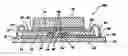
DETAILED DESCRIPTION OF THE INVENTIONFIG. 1 illustrates a first embodiment of the present invention designated as a flip-chip style/flip-chip attachment assembly 100. Assembly 100 comprises a semiconductor die 12 having an inverted active surface 14 with at least one flip-chip electric connection 16 (such as a C4 solder bump connection, a pin connection, or a surface mount J-lead connection, by way of example) extending substantially perpendicularly from a bond pad 15 on the semiconductor die active surface 14. The flip-chip electric connections 16 are attached to an upper surface 20 of an adaptor board 18 in such a manner that the flip-chip electric connections 16 make electrical contact with electrical contact elements 21 in or on the surface of adaptor board 18. The electrical contact elements 21 make electrical communication between each flip-chip electric connection 16, through circuit traces 23 (exemplary traces shown in broken lines) in the adaptor board 18, to at least one master board connector 22 extending substantially perpendicularly from a lower surface 24 of the adaptor board 18 to connect adaptor board 18 to an aligned terminal 31 on master board 30. Preferably, a sealing compound 26 is disposed between the semiconductor die 12 and the adaptor board 18 to prevent contamination of the flip-chip electric connections 16 and to more firmly secure semiconductor die 12 to adaptor board 18.
In actual practice, there will be a plurality of terminals 31 arranged in a specific, perhaps industry-standard pattern, on master board 30, and master board connectors will be arranged in a mirror-image pattern to terminals 31 for mating connection therewith. Master board connectors 22 and terminals 31 may comprise any electrical connection mechanism known in the art, in addition to those previously described herein.
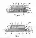
FIGS. 2 and 2A illustrate a second embodiment of the present invention designated as a flip-chip style/wire bond attachment assembly 200. Components common to both FIG. 1 and FIG. 2 retain the same numeric designation. The assembly 200 comprises the semiconductor die 12 having active surface 14 with at least one flip-chip electric connection 16, as known in the art, extending substantially perpendicularly from a bond pad 15 on the semiconductor die active surface 14. The flip-chip electric connections 16 are attached to the adaptor board upper surface 20 in such a manner that the flip-chip electric connections 16 make electrical contact with electrical contact elements 21 on the adaptor board 18. The electrical contact elements 21 communicate between each flip-chip electric connection 16 to bond pads 28 on the adaptor board upper surface 20 through circuit traces 23. The adaptor board lower surface 24 is bonded to an upper surface 36 of a master board 30 with an adhesive 32, which may comprise a liquid or gel adhesive, or an adhesive tape, all as known in the art. If desired, adhesive 32 may be a heat-conductive adhesive. A wire bond 34 extends from each adaptor board bond pad 28 to a corresponding bond pad or lead end 35 on the upper surface 36 of master board 30, bond pad or lead end 35 communicating with other components mounted to master board 30 or with other components on other boards or other assemblies through circuit traces or other conductors known in the art.
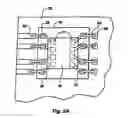
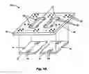
FIGS. 3 and 3A illustrate a third embodiment of the present invention designated as a wire bond style/flip-chip attachment assembly 300. Components which are common to the previous figures retain the same numeric designation. The assembly 300 comprises an inverted semiconductor die 12 having active surface 14 with at least one bond pad 38 on the semiconductor die active surface 14. As illustrated, the bond pads 38 are arranged in two rows extending down the longitudinal axis of semiconductor die 12 being located transverse to the plane of the page, such an arrangement commonly being used for a “leads over” connection to frame leads extending over the die in its normal, upright position. The semiconductor die active surface 14 is bonded to the adaptor board upper surface 20 with an insulating, sealing adhesive 40. The adaptor board 18 includes at least one or more wire bond vias 42 which is located in a position or positions aligned with the semiconductor die bond pads 38. Each individual wire bond 134 is connected to each corresponding individual semiconductor die bond pad 38. Each wire bond 134 extends from the semiconductor die bond pad 38 to a corresponding bond pad or lead 39 on the adaptor board lower surface 24, which communicates with master board connectors 22 through circuit traces 23. The master board terminals 31 are in electrical communication with at least one master board connector 22 extending substantially perpendicularly from the adaptor board lower surface 24. Preferably, a sealant 44 encases the bond wires 134 and seals the wire bond via 42 to prevent contamination and damage to the wire bonds.
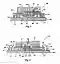
FIG. 4 illustrates a fourth embodiment of the present invention designated as a wire bond style/wire bond attachment assembly 400. Components which are common to the previous figures retain the same numeric designation. The assembly 400 comprises the semiconductor die 12 having active surface 14 with at least one bond pad 38 on the semiconductor die active surface 14. As with the embodiment of FIG. 3, semiconductor die 12 in this instance employs bond pads 38 in a “leads over” configuration. The semiconductor die active surface 14 is bonded to the adaptor board upper surface 20 with an insulating, sealing adhesive 40. The adaptor board 18 includes at least one wire bond via 42 which is located in a position or positions aligned with the semiconductor die bond pads 38. Each individual wire bond 134 is connected to each corresponding semiconductor die bond pad 38. Each wire bond 134 extends from the semiconductor die bond pad 38 to a corresponding bond pad 46 within the wire bond via 42. The via bond pads 46 are in electrical communication through circuit traces 23 with at least one corresponding adaptor board bond pad 28. The adaptor board lower surface 24 is bonded to the master board upper surface 36 with the adhesive 32. Wire bonds 34 extend from the adapter board upper surface 20 to a corresponding bond pad or lead on the master board upper surface 36. Preferably, the wire bond via sealant 44 encases the bond wires 134 and seals the wire bond via 42 to prevent contamination.
Having thus described in detail preferred embodiments of the present invention, it is to be understood that the invention defined by the appended claims is not to be limited by particular details set forth in the above description as many apparent variations thereof are possible without departing from the spirit or scope thereof.
Claims
What is claimed is:1. A method for forming a stackable ball grid array package, comprising:
providing a substrate having a first surface for receiving a semiconductor die and having an opposing second surface and having an aperture;
patterning conductors on the second surface to provide conductive paths between terminal pads located near the aperture and conductive element pads located near the periphery of the substrate;
mounting a semiconductor˜die on the first surface at least partially over the aperture, the die having one or more bond pads located over the aperture;
connecting one or more bond pads of the semiconductor die to one of the terminal pads by a bond wire extending through the aperture;
providing a material covering the bond wire and that portion of the semiconductor die overlying the aperture, the material having a first profile height with respect to the second surface; and
providing one or more conductive elements disposed on the conductive element pads, the conductive elements having a second profile height with respect to the second surface that is greater than the first profile height.
2. The method of claim 1, wherein providing one or more conductive elements further comprises placing solder balls on the conductive element pads, and reflowing the solder balls to attach them to the conductive element pads.
3. The method of claim 1, wherein mounting a semiconductor die further comprises providing a die attach pad on the first surface of the substrate, the die attach pad being a dielectric material having an opening corresponding to the aperture in the substrate.
4. The method of claim 3, wherein providing a die attach pad further comprises providing an epoxy resin.
5. The method of claim 3, wherein providing a die attach pad further comprises providing an adhesively coated dielectric tape.
6. The method of claim 1, wherein providing a substrate further comprises providing isolated conductive element pads on the substrate for receiving additional conductive elements at locations isolated from the conductive traces on the substrate.
7. The method of claim 6, wherein providing a substrate further comprises forming conductive vias between the first surface and the second surface.
8. The method of claim 7, wherein providing a substrate further comprises forming conductors on the first surface.
9. The method of claim 8, wherein providing a substrate further comprises forming conductive element pads on the first surface.
10. The method of claim 9, wherein providing a substrate further comprises providing conductive elements on the conductive element pads of the first surface.
11. The method of claim 10 and further comprising coupling at least one of the conductive elements on the first surface to a conductor on the first surface.
12. The method of claim 11, and further comprising coupling at least one conductive element on the first surface to a conductor on the first surface, to one of the conductive vias through the substrate, to a conductive trace on the second surface, and to a conductive element on the second surface.
13. The method of claim 12, wherein providing conductive elements on the first surface further comprises placing one or more solder balls on the conductive element pads on the first surface.
14. The method of claim 1, wherein the semiconductor die has a periphery and the conductive element pads are located outside of that periphery.
15. The method of claim 1, wherein the semiconductor die has a periphery and the conductive element pads are located within that periphery.
Images & Drawings included:
Sources:
- United States Patent and Trademark Office - verify current appl. status at the USPTO↗
Similar patent applications:
- » 9699537
Flip-chip adaptor package for bare die - » 20050167850
Flip-chip adaptor package for bare die
Recent applications in this class:
- » 20250273622 2025-08-28
ELECTRONIC PACKAGE AND MANUFACTURING METHOD THEREOF - » 20250266391 2025-08-21
LASER ASSISTED BONDING METHOD - » 20250259964 2025-08-14
MOLDED SPACER FOR SURFACE MOUNT TECHNOLOGY - » 20250246576 2025-07-31
ELECTRONIC DEVICE AND A METHOD FOR FORMING THE SAME - » 20250226358 2025-07-10
PRE-ATTACHED ENGINEERED SOLDERS FOR ULTRA-LOW RESIDUE SOLDERING - » 20250226357 2025-07-10
ELECTRICAL CIRCUIT FORMATION METHOD AND ELECTRICAL CIRCUIT FORMATION DEVICE - » 20250219019 2025-07-03
SEMICONDUCTOR DEVICE AND METHOD FOR MANUFACTURING THE SAME - » 20250219018 2025-07-03
SEMICONDUCTOR PACKAGING METHOD, SEMICONDUCTOR ASSEMBLY COMPONENT AND ELECTRONIC DEVICE - » 20250219017 2025-07-03
DIE-BONDING METHOD FOR PREVENTING DIE FROM BENDING - » 20250210584 2025-06-26
METHOD OF BONDING LIGHT EMITTING ELEMENT AND METHOD OF MANUFACTURING DISPLAY DEVICE, HAVING THE SAME
Recent applications for this Assignee:
- » 20250294729 2025-09-18
Memory Circuitry And Methods Used In Forming Memory Circuitry - » 20250293722 2025-09-18
HIGH SPEED RECEIVER FOR MULTI-GIGA HERTZ OPERATIONS - » 20250292844 2025-09-18
Validating Uninitialized Usage-Based-Disturbance Data - » 20250292836 2025-09-18
Memory Arrays Comprising Strings Of Memory Cells And Methods Used In Forming A Memory Array Comprising Strings Of Memory Cells - » 20250292835 2025-09-18
Memory Arrays Comprising Strings Of Memory Cells And Methods Used In Forming A Memory Array Comprising Strings Of Memory Cells - » 20250292821 2025-09-18
Multiple-Row Refresh for Usage-Based Disturbance Mitigation - » 20250291671 2025-09-18
APPARATUSES AND METHODS FOR ADJUSTING REFRESH RATES ON MEMORY DEVICES OF A MODULE - » 20250284540 2025-09-11
Broadcasting a Host-Controlled Parameter to Circuitry Distributed at a Local-Bank Level for Usage-Based-Disturbance Mitigation - » 20250280546 2025-09-04
Integrated Circuitry, Array of Cross-Point Memory Cells, Method Used in Forming Integrated Circuitry - » 20250280539 2025-09-04
Integrated Circuitry Comprising a Memory Array Comprising Strings of Memory Cells and Methods Used in Forming a Memory Array Comprising Strings of Memory Cells