Method for manufacturing tight pitch, flip chip integrated circuit packages
US20100314433A1
2010-12-16
12/482,668
2009-06-11
✅ Patent granted
US 8,371,497 B2
2013-02-12
-
-
Devang R Patel
Michelle Gallardo | Nicholas J. Pauley | Jonathan T. Velasco
2029-07-08
Abstract:
A flip chip packaging method to attach a die to a package substrate, the method including dipping the die into solder paste; placing the die onto the package substrate; and reflowing the solder paste to attach the die to the package substrate. Other embodiments are described and claimed.
Assignee:
- QUALCOMM INCORPORATED 41,536 🇺🇸 San Diego, CA, United States
Applicant:
Interested in similar patents?
Get notified when new applications in this technology area are published.
Classification:
H01L24/16 » CPC main
Arrangements for connecting or disconnecting semiconductor or solid-state bodies; Methods or apparatus related thereto; Means for bonding being attached to, or being formed on, the surface to be connected, e.g. chip-to-package, die-attach, "first-level" interconnects; Manufacturing methods related thereto; Bump connectors ; Manufacturing methods related thereto; Structure, shape, material or disposition of the bump connectors after the connecting process of an individual bump connector
H01L21/4867 » CPC further
Processes or apparatus adapted for the manufacture or treatment of semiconductor or solid state devices or of parts thereof; Manufacture or treatment of semiconductor devices or of parts thereof the devices having at least one potential-jump barrier or surface barrier, e.g. PN junction, depletion layer or carrier concentration layer; Manufacture or treatment of parts, e.g. containers, prior to assembly of the devices, using processes not provided for in a single one of the subgroups -; Conductive parts; Leads on or in insulating or insulated substrates, e.g. metallisation Applying pastes or inks, e.g. screen printing
H01L21/6835 » CPC further
Processes or apparatus adapted for the manufacture or treatment of semiconductor or solid state devices or of parts thereof; Apparatus specially adapted for handling semiconductor or electric solid state devices during manufacture or treatment thereof; Apparatus specially adapted for handling wafers during manufacture or treatment of semiconductor or electric solid state devices or components ; Apparatus not specifically provided for elsewhere for supporting or gripping using temporarily an auxiliary support
H01L24/11 » CPC further
Arrangements for connecting or disconnecting semiconductor or solid-state bodies; Methods or apparatus related thereto; Means for bonding being attached to, or being formed on, the surface to be connected, e.g. chip-to-package, die-attach, "first-level" interconnects; Manufacturing methods related thereto; Bump connectors ; Manufacturing methods related thereto Manufacturing methods
H01L24/81 » CPC further
Arrangements for connecting or disconnecting semiconductor or solid-state bodies; Methods or apparatus related thereto; Methods for connecting semiconductor or other solid state bodies using means for bonding being attached to, or being formed on, the surface to be connected using a bump connector
H01L24/75 » CPC further
Arrangements for connecting or disconnecting semiconductor or solid-state bodies; Methods or apparatus related thereto; Apparatus for manufacturing arrangements for connecting or disconnecting semiconductor or solid-state bodies Apparatus for connecting with bump connectors or layer connectors
H01L2224/11003 » CPC further
Indexing scheme for arrangements for connecting or disconnecting semiconductor or solid-state bodies and methods related thereto as covered by; Means for bonding being attached to, or being formed on, the surface to be connected, e.g. chip-to-package, die-attach, "first-level" interconnects; Manufacturing methods related thereto; Bump connectors; Manufacturing methods related thereto; Manufacturing methods; Involving a temporary auxiliary member not forming part of the manufacturing apparatus, e.g. removable or sacrificial coating, film or substrate for holding or transferring the bump preform
H01L2224/1131 » CPC further
Indexing scheme for arrangements for connecting or disconnecting semiconductor or solid-state bodies and methods related thereto as covered by; Means for bonding being attached to, or being formed on, the surface to be connected, e.g. chip-to-package, die-attach, "first-level" interconnects; Manufacturing methods related thereto; Bump connectors; Manufacturing methods related thereto; Manufacturing methods by local deposition of the material of the bump connector in liquid form
H01L2224/1182 » CPC further
Indexing scheme for arrangements for connecting or disconnecting semiconductor or solid-state bodies and methods related thereto as covered by; Means for bonding being attached to, or being formed on, the surface to be connected, e.g. chip-to-package, die-attach, "first-level" interconnects; Manufacturing methods related thereto; Bump connectors; Manufacturing methods related thereto; Manufacturing methods; Post-treatment of the bump connector Applying permanent coating, e.g. in-situ coating
H01L2224/11822 » CPC further
Indexing scheme for arrangements for connecting or disconnecting semiconductor or solid-state bodies and methods related thereto as covered by; Means for bonding being attached to, or being formed on, the surface to be connected, e.g. chip-to-package, die-attach, "first-level" interconnects; Manufacturing methods related thereto; Bump connectors; Manufacturing methods related thereto; Manufacturing methods; Post-treatment of the bump connector; Applying permanent coating, e.g. in-situ coating by dipping, e.g. in a solder bath
H01L2224/13099 » CPC further
Indexing scheme for arrangements for connecting or disconnecting semiconductor or solid-state bodies and methods related thereto as covered by; Means for bonding being attached to, or being formed on, the surface to be connected, e.g. chip-to-package, die-attach, "first-level" interconnects; Manufacturing methods related thereto; Bump connectors; Manufacturing methods related thereto; Structure, shape, material or disposition of the bump connectors prior to the connecting process of an individual bump connector; Core members of the bump connector Material
H01L2224/75 » CPC further
Indexing scheme for arrangements for connecting or disconnecting semiconductor or solid-state bodies and methods related thereto as covered by; Apparatus for manufacturing arrangements for connecting or disconnecting semiconductor or solid-state bodies and for methods related thereto Apparatus for connecting with bump connectors or layer connectors
H01L2224/7515 » CPC further
Indexing scheme for arrangements for connecting or disconnecting semiconductor or solid-state bodies and methods related thereto as covered by; Apparatus for manufacturing arrangements for connecting or disconnecting semiconductor or solid-state bodies and for methods related thereto; Apparatus for connecting with bump connectors or layer connectors Means for applying permanent coating, e.g. in-situ coating
H01L2224/75611 » CPC further
Indexing scheme for arrangements for connecting or disconnecting semiconductor or solid-state bodies and methods related thereto as covered by; Apparatus for manufacturing arrangements for connecting or disconnecting semiconductor or solid-state bodies and for methods related thereto; Apparatus for connecting with bump connectors or layer connectors; Means for supplying the connector to be connected in the bonding apparatus Feeding means
H01L2224/7901 » CPC further
Indexing scheme for arrangements for connecting or disconnecting semiconductor or solid-state bodies and methods related thereto as covered by; Apparatus for manufacturing arrangements for connecting or disconnecting semiconductor or solid-state bodies and for methods related thereto; Apparatus for Tape Automated Bonding [TAB] Means for cleaning, e.g. brushes, for hydro blasting, for ultrasonic cleaning, for dry ice blasting, using gas-flow, by etching, by applying flux or plasma
H01L2224/81011 » CPC further
Indexing scheme for arrangements for connecting or disconnecting semiconductor or solid-state bodies and methods related thereto as covered by; Methods for connecting semiconductor or other solid state bodies using means for bonding being attached to, or being formed on, the surface to be connected using a bump connector; Pre-treatment of the bump connector or the bonding area; Cleaning the bump connector, e.g. oxide removal step, desmearing Chemical cleaning, e.g. etching, flux
H01L2224/8102 » CPC further
Indexing scheme for arrangements for connecting or disconnecting semiconductor or solid-state bodies and methods related thereto as covered by; Methods for connecting semiconductor or other solid state bodies using means for bonding being attached to, or being formed on, the surface to be connected using a bump connector; Pre-treatment of the bump connector or the bonding area Applying permanent coating to the bump connector in the bonding apparatus, e.g. in-situ coating
H01L2224/81024 » CPC further
Indexing scheme for arrangements for connecting or disconnecting semiconductor or solid-state bodies and methods related thereto as covered by; Methods for connecting semiconductor or other solid state bodies using means for bonding being attached to, or being formed on, the surface to be connected using a bump connector; Pre-treatment of the bump connector or the bonding area Applying flux to the bonding area
H01L2224/81191 » CPC further
Indexing scheme for arrangements for connecting or disconnecting semiconductor or solid-state bodies and methods related thereto as covered by; Methods for connecting semiconductor or other solid state bodies using means for bonding being attached to, or being formed on, the surface to be connected using a bump connector; Arrangement of the bump connectors prior to mounting wherein the bump connectors are disposed only on the semiconductor or solid-state body
H01L2224/81815 » CPC further
Indexing scheme for arrangements for connecting or disconnecting semiconductor or solid-state bodies and methods related thereto as covered by; Methods for connecting semiconductor or other solid state bodies using means for bonding being attached to, or being formed on, the surface to be connected using a bump connector; Bonding techniques; Soldering or alloying Reflow soldering
H01L2924/01005 » CPC further
Indexing scheme for arrangements or methods for connecting or disconnecting semiconductor or solid-state bodies as covered by; Chemical elements Boron [B]
H01L2924/01006 » CPC further
Indexing scheme for arrangements or methods for connecting or disconnecting semiconductor or solid-state bodies as covered by; Chemical elements Carbon [C]
H01L2924/01033 » CPC further
Indexing scheme for arrangements or methods for connecting or disconnecting semiconductor or solid-state bodies as covered by; Chemical elements Arsenic [As]
H01L2924/01075 » CPC further
Indexing scheme for arrangements or methods for connecting or disconnecting semiconductor or solid-state bodies as covered by; Chemical elements Rhenium [Re]
H01L2924/01082 » CPC further
Indexing scheme for arrangements or methods for connecting or disconnecting semiconductor or solid-state bodies as covered by; Chemical elements Lead [Pb]
H01L2924/014 » CPC further
Indexing scheme for arrangements or methods for connecting or disconnecting semiconductor or solid-state bodies as covered by; Alloys Solder alloys
H01L2924/14 » CPC further
Indexing scheme for arrangements or methods for connecting or disconnecting semiconductor or solid-state bodies as covered by; Details of semiconductor or other solid state devices to be connected; Device type Integrated circuits
H01L2924/00014 » CPC further
Indexing scheme for arrangements or methods for connecting or disconnecting semiconductor or solid-state bodies as covered by; Technical content checked by a classifier the subject-matter covered by the group, the symbol of which is combined with the symbol of this group, being disclosed without further technical details
H01L2924/00011 » CPC further
Indexing scheme for arrangements or methods for connecting or disconnecting semiconductor or solid-state bodies as covered by; Technical content checked by a classifier Not relevant to the scope of the group, the symbol of which is combined with the symbol of this group
H01L2224/0401 » CPC further
Indexing scheme for arrangements for connecting or disconnecting semiconductor or solid-state bodies and methods related thereto as covered by; Means for bonding being attached to, or being formed on, the surface to be connected, e.g. chip-to-package, die-attach, "first-level" interconnects; Manufacturing methods related thereto; Bonding areas; Manufacturing methods related thereto; Structure, shape, material or disposition of the bonding areas prior to the connecting process Bonding areas specifically adapted for bump connectors, e.g. under bump metallisation [UBM]
B23K31/02 IPC
Processes relevant to this subclass, specially adapted for particular articles or purposes, but not covered by only one of the preceding main groups relating to soldering or welding
B23K35/34 IPC
Rods, electrodes, materials, or media, for use in soldering, welding, or cutting characterised by the composition or nature of the material comprising compounds which yield metals when heated
Description
FIELD
The present invention relates to packaging of integrated circuits, and more particularly to flip chip integrated circuit packages.
BACKGROUND
In a flip chip packaged integrated circuit, or simply “flip chip” for short, a die (chip) containing the integrated circuit has its active side facing a package substrate. In the flip chip process, also formally called the Controlled Collapse Chip Connection (C4) evaporative bump process, conductive bumps are formed and soldered to pads on the active side. The solder bumped die is then placed face down onto matching bonding pads on a multilayer organic package substrate. The assembly is reflowed so that the conductive bumps are soldered to pads on the package substrate to provide electrical connection between the active side of the integrated circuit and the package substrate. This electrical connection forms part of the so-called level 1 interconnect. The conductive bumps also provide a load bearing link between the die and the package substrate. Usually, the conductive bumps comprise solder.
After the die is attached to the substrate, an epoxy resin (or underfill) is usually applied at the interface between the die and the package substrate to help compensate for the difference in the coefficient of thermal expansion (CTE) between the die and the package substrate, and to prevent moisture from getting to the die surface. The flip chip may also be capped with a liquid epoxy for further protection.
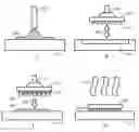
FIG. 1 illustrates in simplified form a process comprising three steps to attach and solder the conductive bumps on a flip chip die to the package substrate, where the steps are labeled in sequential order as “A”, “B”, and “C”. In step A, die 102 held by tool 104 is dipped into flux resin 106. Arrow 108 pictorially represents this dipping process, where conductive bumps 110 are dipped into flux resin 106 and then pulled out. In step B, the numeric label 112 denotes solder wetting conductive bumps 110. Arrow 114 pictorially represents die 102 being placed onto package substrate 116. In step C, wavy lines 118 pictorially represent heat being applied to cause reflow of the solder so that conductive bumps 110 are soldered to pads (not shown) on package substrate 116.
As integrated circuits become more complex with higher numbers of input and output pads with a corresponding increase in the number of conductive bumps, the pitch of the conductive bumps is expected to increase. However, some problems that may arise with a tighter pitch using a reflow and attach process such as that illustrated in FIG. 1 are, to name just a few: opens or shorts leading to lower yield, poor wettability of the solder on the conductive bumps, and electrical connections between conductive bumps and pads that may fail over time. Warping of the die and package substrate may increase the likelihood of these problems.
A low cost manufacturing process to attach a die to a package substrate resulting in good yield and reliability in a tight pitch, flip chip integrated package is of utility.
SUMMARY
In an embodiment, a die is dipped into solder paste, placed onto a package substrate, and then the solder paste is reflowed to attach the die to the package substrate.
In another embodiment, to attach a die to a package substrate, solder paste is applied to the package substrate, the die is placed onto the package substrate before reflow of the solder paste; and then the solder paste is reflowed to attach the die to the package substrate.
In another embodiment, to attach a die to a package substrate, solder paste is dispensed onto pads on the package substrate, the die is placed onto the package substrate before reflow of the solder paste, and then the solder paste is reflowed to attach the die to the package substrate.
BRIEF DESCRIPTION OF THE DRAWINGS
FIG. 1 illustrates a conventional process in flip chip manufacturing.
FIG. 2 illustrates a process to attach and solder the conductive bumps on a die to pads on a package substrate according to an embodiment.
FIG. 3 illustrates a process to attach and solder the conductive bumps on a die to pads on a package substrate according to another embodiment.
FIG. 4 illustrates a process to attach and solder the conductive bumps on a die to pads on a package substrate according to another embodiment.
DESCRIPTION OF EMBODIMENTS
In the description that follows, the scope of the term “some embodiments” is not to be so limited as to mean more than one embodiment, but rather, the scope may include one embodiment, more than one embodiment, or perhaps all embodiments.
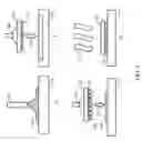
FIG. 2 illustrates a process to attach and solder the conductive bumps on a die to pads on a package substrate according to an embodiment, with sub-figures in FIG. 2 labeled as “A”, “B”, “C”, and “D”, where these labels do not necessarily imply a sequential order. For example, the process illustrated as “A” in FIG. 2 need not be part of an embodiment, or if it is to be included in an embodiment, then it need not necessarily be performed before the process labeled as “B”.
In “A” of FIG. 2, a jet flux process is used whereby tool 202 applies (e.g., sprays) flux resin 204 onto package substrate 116. In “B” of FIG. 2, die 102 is dipped into solder paste 206 and then removed, where arrow 208 pictorially represents this dipping process. Solder paste 206 may be, for example, a combination of flux and particulate solder. In the dipping process in “B”, the bottom portions of conductive bumps 110 are put into contact with solder paste 206 such that when tool 104 removes conductive bumps 110 from solder paste 206, there is no wetting between conductive bumps 110 that may lead to shorts. Sub-figure “C” of FIG. 2 illustrates solder paste 206 wetting the bottom surfaces of conductive bumps 110, such that there is no bridging of solder between the conductive bumps to cause a short. Arrow 212 pictorially represents placing die 102 onto package substrate 116.
If the process indicated in “A” of FIG. 2 is performed, then flux resin 204 is already on package substrate 116 in the process of “C”, but for some embodiments the process indicated by “A” in FIG. 2 may not be performed so that flux resin 204 may not be present on package substrate 116 in the process of “C”. For some embodiments, flux resin 204 may have a thickness of around 5 to 15 μm. The use of flux resin 204 may increase the wettability of solder paste 206 when the process “C” in FIG. 2 is performed.
In “D” of FIG. 2, wavy lines 118 pictorially represent applying heat so as to reflow solder paste 206 in order to solder and attach conductive bumps 110 to pads (not shown) on package substrate 116.
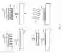
FIG. 3 illustrates a process to attach and solder the conductive bumps on a die to pads on a package substrate according to another embodiment. Sub-figures in FIG. 3 are labeled as “A”, “B”, “C”, and “D”, where the alphabetical order of these labels implies a sequential order. In process “A” of FIG. 3, tool 302 comprising multiple needles 304 is dipped into solder paste 206 and then removed, as pictorially represented by arrow 306. Needles 304 have the same array pattern as conductive bumps 110 on die 102.
In process “B” of FIG. 3, solder paste 206 wets the tips of needles 304, where arrow 308 pictorially represents placing the tips of needles 304 close to package substrate 116 to dispense solder paste 206 onto package substrate 116.
Process “C” of FIG. 3 illustrates that solder paste 206 has been dispensed onto package substrate 116 to form drops of solder paste 206 at the same pitch as conductive bumps 110. Arrow 310 pictorially represents placing die 102 onto package substrate 116 so that conductive bumps 110 come into contact with corresponding drops of solder paste 206.
In process “D” of FIG. 3, wavy lines 118 pictorially represent the application of heat to cause reflow of solder paste 206 so that conductive bumps 110 are soldered to pads (not shown) on package substrate 116.
FIG. 4 illustrates a process to attach and solder the conductive bumps on a die to pads on a package substrate according to another embodiment. Sub-figures in FIG. 4 are labeled as “A”, “B”, and “C”, where the alphabetical order of these labels implies a sequential order. In process “A” of FIG. 4, tool 402 comprising multiple needles 404 dispenses solder paste 206 onto pads 405 on package substrate 116. Needles 404 have small openings at their tips so that when under pressure, solder paste 206 flows through these openings so that drops of solder paste 206 may be dispensed onto pads 405 on package substrate 116. The process of bringing tool 402 close to package substrate 116, dispensing solder paste 206, and bringing tool 402 away is pictorially represented by arrow 406. Needles 404 have the same array pattern as conductive bumps 110 on die 102.
Processes “B” and “C” in FIG. 4 are the same, respectively, as processes “C” and “D” in FIG. 3, so that part of the description for the embodiment of FIG. 3 need not be repeated with respect to FIG. 4. (For ease of illustration, pads 405 are now shown in processes “B” and “C” of FIG. 4.)
Additional processes well known in the technology of flip chip packaging, such as applying underfill to the interface between die 102 and package substrate 116 in FIGS. 2, 3, and 4, may be performed, but are not shown in these figures for ease of illustration. Also, pads, under bump metallization layers, and other protective layers, such as for example oxide surface protectant layers, are well known but are not shown in all or some of these figures for ease of illustration.
Various modifications may be made to the described embodiments without departing from the scope of the invention as claimed below.
Claims
1. A method to attach a die to a package substrate, the method comprising:
applying flux resin to the package substrate;
dipping at least a portion of the die into solder paste within a solder paste container;
placing the dipped die onto the package substrate after applying the flux resin; and
reflowing the solder paste remaining on the portion of the die to attach the die to the package substrate.
2. The method of claim 1, wherein the die has conductive bumps, and wherein dipping the die into the solder paste comprises dipping the conductive bumps into the solder paste.
3. The method of claim 2, wherein the package substrate has pads, and wherein reflowing the solder paste to attach the die to the package substrate comprises soldering the conductive bumps to the pads.
4. The method of claim 1, wherein the package substrate has pads, wherein the die has conductive bumps, and wherein reflowing the solder paste to attach the die to the package substrate comprises soldering the conductive bumps to the pads.
5-18. (canceled)
19. The method of claim 1, wherein the solder paste is a combination of flux and particulate solder.
20. The method of claim 1, wherein the flux resin has a thickness in the range of 5 micrometers and 15 micrometers.
21. The method of claim 2, wherein there is no wetting between the conductive bumps.
22. The method of claim 2, wherein only a bottom portion of the conductive bumps is dipped into the solder paste within the solder paste container.
23. A packaged die prepared by a process comprising the steps of:
applying flux resin to a package substrate;
dipping at least a portion of a die into solder paste within a solder paste container;
removing the die from the solder paste container;
placing the dipped die onto the package substrate after applying the flux resin; and
reflowing the solder paste remaining on the portion of the die to attach the die to the package substrate.
24. The packaged die of claim 23, wherein the die has conductive bumps, and wherein dipping the die into the solder paste comprises dipping the conductive bumps into the solder paste.
25. The packaged die of claim 24, wherein the package substrate has pads, and wherein reflowing the solder paste to attach the die to the package substrate comprises soldering the conductive bumps to the pads.
26. The packaged die of claim 23, wherein the package substrate has pads, wherein the die has conductive bumps, and wherein reflowing the solder paste to attach the die to the package substrate comprises soldering the conductive bumps to the pads.
27. A method to attach a die to a package substrate, the method comprising:
a step for applying flux resin to the package substrate;
a step for dipping at least a portion of the die into solder paste within a solder paste container;
a step for placing the dipped die onto the package substrate after applying the flux resin; and
a step for reflowing the solder paste remaining on the portion of the die to attach the die to the package substrate.
28. The method of claim 27, wherein the die has conductive bumps, and wherein dipping the die into the solder paste comprises dipping the conductive bumps into the solder paste.
29. The method of claim 28, wherein the package substrate has pads, and wherein reflowing the solder paste to attach the die to the package substrate comprises soldering the conductive bumps to the pads.
30. The method of claim 28, wherein there is no wetting between the conductive bumps.
31. The method of claim 28, wherein only a bottom portion of the conductive bumps is dipped into the solder paste within the solder paste container.
30. The method of claim 27, wherein the flux resin has a thickness in the range of 5 micrometers and 15 micrometers.
33. The method of claim 27, wherein the package substrate has pads, wherein the die has conductive bumps, and wherein reflowing the solder paste to attach the die to the package substrate comprises soldering the conductive bumps to the pads.
34. The method of claim 27, wherein each of steps are performed by a processor integrated into an electronic device.
Images & Drawings included:


Sources:
- United States Patent and Trademark Office - verify current appl. status at the USPTO↗
Recent applications in this class:
- » 20250279381 2025-09-04
SEMICONDUCTOR DIE HAVING A DIE LEVEL DISTRIBUTION (DLD) METALLIZATION STRUCTURE INCLUDING A METAL PAD AND A SHORTER VIA COUPLING THE METAL PAD TO A METAL INTERCONNECT IN THE DIE FOR IMPROVED SIGNAL PATH CONDUCTIVITY - » 20250246569 2025-07-31
STACKED INTEGRATED CIRCUIT DEVICES WITH FACE-TO-FACE CONNECTIONS BETWEEN LOGIC AND MEMORY DIES - » 20250239554 2025-07-24
SEMICONDUCTOR PACKAGE - » 20250219001 2025-07-03
SEMICONDUCTOR PACKAGE AND METHOD FOR MAKING THE SAME - » 20250219000 2025-07-03
SEMICONDUCTOR PACKAGE - » 20250218999 2025-07-03
PASSIVE COMPONENT ASSEMBLY FOR THICKNESS MODIFICATION TO MATCH CORE THICKNESS - » 20250210563 2025-06-26
SEMICONDUCTOR DEVICE - » 20250210562 2025-06-26
PILLARS AS STOPS FOR PRECISE CHIP-TO-CHIP SEPARATION - » 20250210561 2025-06-26
BONDED STRUCTURE - » 20250210560 2025-06-26
SEMICONDUCTOR PACKAGE AND METHOD FOR MANUFACTURING THE SAME
Recent applications for this Assignee:
- » 20250267371 2025-08-21
ADAPTIVE SYNCHRONIZATION FOR AUTOMATIC EXPOSURE CONTROL (AEC) - » 20250264908 2025-08-21
READ SYNCHRONIZATION DELAY AT SUBORDINATE DEVICE FOR 1 WIRE PROTOCOL - » 20250260602 2025-08-14
SPUR DETECTION, ESTIMATION, AND MITIGATION - » 20250238104 2025-07-24
DEVICES INCLUDING ONE OR MORE HIGH-IMPEDANCE LAYERS BETWEEN A DISPLAY STACK AND AN ULTRASONIC FINGERPRINT SENSOR STACK - » 20250233826 2025-07-17
Prioritizing Data Flows - » 20250233642 2025-07-17
ANTENNA PANEL DISPLACEMENT - » 20250233623 2025-07-17
GEOMETRIC DEEP LEARNING FOR LATTICE REDUCTION - » 20250227008 2025-07-10
ANTENNA ELEMENT CALIBRATION ALGORITHM - » 20250226858 2025-07-10
UPLINK MULTI-USER MULTIPLE-INPUT MULTIPLE-OUTPUT (UL MU-MIMO) PRECODING USING PER-STATION FEEDBACK - » 20250225078 2025-07-10
Systems And Methods For Dynamically Allocating Memory Pages To Enable Memory Footprint Reduction