Integrated circuit including bond wire directly bonded to pad
US20110260307A1
2011-10-27
12/768,134
2010-04-27
✅ Patent granted
US 8,432,024 B2
2013-04-30
-
-
David S Blum
Dicke, Billig & Czaja, PLLC
2030-12-03
Abstract:
An integrated circuit includes a chip including a copper bond pad metallization, and a copper bond wire including a copper ball. The copper ball is bonded directly to the copper bond pad.
Assignee:
- INFINEON TECHNOLOGIES AG 8,942 🇩🇪 Neubiberg, Germany
Applicant:
Interested in similar patents?
Get notified when new applications in this technology area are published.
Classification:
H01L23/3735 » CPC main
Details of semiconductor or other solid state devices; Arrangements for cooling, heating, ventilating or temperature compensation ; Temperature sensing arrangements; Selection of materials, or shaping, to facilitate cooling or heating, e.g. heatsinks; Cooling facilitated by selection of materials for the device or materials for thermal expansion adaptation, e.g. carbon Laminates or multilayers, e.g. direct bond copper ceramic substrates
H01L24/05 » CPC further
Arrangements for connecting or disconnecting semiconductor or solid-state bodies; Methods or apparatus related thereto; Means for bonding being attached to, or being formed on, the surface to be connected, e.g. chip-to-package, die-attach, "first-level" interconnects; Manufacturing methods related thereto; Bonding areas ; Manufacturing methods related thereto; Structure, shape, material or disposition of the bonding areas prior to the connecting process of an individual bonding area
H01L24/48 » CPC further
Arrangements for connecting or disconnecting semiconductor or solid-state bodies; Methods or apparatus related thereto; Means for bonding being attached to, or being formed on, the surface to be connected, e.g. chip-to-package, die-attach, "first-level" interconnects; Manufacturing methods related thereto; Wire connectors; Manufacturing methods related thereto; Structure, shape, material or disposition of the wire connectors after the connecting process of an individual wire connector
H01L24/85 » CPC further
Arrangements for connecting or disconnecting semiconductor or solid-state bodies; Methods or apparatus related thereto; Methods for connecting semiconductor or other solid state bodies using means for bonding being attached to, or being formed on, the surface to be connected using a wire connector
H01L25/072 » CPC further
Assemblies consisting of a plurality of individual semiconductor or other solid state devices ; Multistep manufacturing processes thereof all the devices being of a type provided for in the same subgroup of groups - , e.g. assemblies of rectifier diodes the devices not having separate containers the devices being of a type provided for in group the devices being arranged next to each other
H01L25/50 » CPC further
Assemblies consisting of a plurality of individual semiconductor or other solid state devices ; Multistep manufacturing processes thereof Multistep manufacturing processes of assemblies consisting of devices, each device being of a type provided for in group or
H01L23/24 » CPC further
Details of semiconductor or other solid state devices; Fillings or auxiliary members in containers or encapsulations , e.g. centering rings; Fillings characterised by the material, its physical or chemical properties, or its arrangement within the complete device solid or gel at the normal operating temperature of the device
H01L23/49568 » CPC further
Details of semiconductor or other solid state devices; Arrangements for conducting electric current to or from the solid state body in operation, e.g. leads, terminal arrangements ; Selection of materials therefor consisting of soldered constructions; Lead-frames or other flat leads specifically adapted to facilitate heat dissipation
H01L23/49582 » CPC further
Details of semiconductor or other solid state devices; Arrangements for conducting electric current to or from the solid state body in operation, e.g. leads, terminal arrangements ; Selection of materials therefor consisting of soldered constructions; Lead-frames or other flat leads characterised by the materials of the lead frames or layers thereon Metallic layers on lead frames
H01L24/29 » CPC further
Arrangements for connecting or disconnecting semiconductor or solid-state bodies; Methods or apparatus related thereto; Means for bonding being attached to, or being formed on, the surface to be connected, e.g. chip-to-package, die-attach, "first-level" interconnects; Manufacturing methods related thereto; Layer connectors, e.g. plate connectors, solder or adhesive layers; Manufacturing methods related thereto; Structure, shape, material or disposition of the layer connectors prior to the connecting process of an individual layer connector
H01L24/32 » CPC further
Arrangements for connecting or disconnecting semiconductor or solid-state bodies; Methods or apparatus related thereto; Means for bonding being attached to, or being formed on, the surface to be connected, e.g. chip-to-package, die-attach, "first-level" interconnects; Manufacturing methods related thereto; Layer connectors, e.g. plate connectors, solder or adhesive layers; Manufacturing methods related thereto; Structure, shape, material or disposition of the layer connectors after the connecting process of an individual layer connector
H01L24/45 » CPC further
Arrangements for connecting or disconnecting semiconductor or solid-state bodies; Methods or apparatus related thereto; Means for bonding being attached to, or being formed on, the surface to be connected, e.g. chip-to-package, die-attach, "first-level" interconnects; Manufacturing methods related thereto; Wire connectors; Manufacturing methods related thereto; Structure, shape, material or disposition of the wire connectors prior to the connecting process of an individual wire connector
H01L24/73 » CPC further
Arrangements for connecting or disconnecting semiconductor or solid-state bodies; Methods or apparatus related thereto Means for bonding being of different types provided for in two or more of groups , , , , , , ,
H01L24/83 » CPC further
Arrangements for connecting or disconnecting semiconductor or solid-state bodies; Methods or apparatus related thereto; Methods for connecting semiconductor or other solid state bodies using means for bonding being attached to, or being formed on, the surface to be connected using a layer connector
H01L2224/04042 » CPC further
Indexing scheme for arrangements for connecting or disconnecting semiconductor or solid-state bodies and methods related thereto as covered by; Means for bonding being attached to, or being formed on, the surface to be connected, e.g. chip-to-package, die-attach, "first-level" interconnects; Manufacturing methods related thereto; Bonding areas; Manufacturing methods related thereto; Structure, shape, material or disposition of the bonding areas prior to the connecting process Bonding areas specifically adapted for wire connectors, e.g. wirebond pads
H01L2224/325 » CPC further
Indexing scheme for arrangements for connecting or disconnecting semiconductor or solid-state bodies and methods related thereto as covered by; Means for bonding being attached to, or being formed on, the surface to be connected, e.g. chip-to-package, die-attach, "first-level" interconnects; Manufacturing methods related thereto; Layer connectors, e.g. plate connectors, solder or adhesive layers; Manufacturing methods related thereto; Structure, shape, material or disposition of the layer connectors after the connecting process of an individual layer connector Material
H01L2224/8382 » CPC further
Indexing scheme for arrangements for connecting or disconnecting semiconductor or solid-state bodies and methods related thereto as covered by; Methods for connecting semiconductor or other solid state bodies using means for bonding being attached to, or being formed on, the surface to be connected using a layer connector; Bonding techniques; Soldering or alloying Diffusion bonding
H01L2224/85045 » CPC further
Indexing scheme for arrangements for connecting or disconnecting semiconductor or solid-state bodies and methods related thereto as covered by; Methods for connecting semiconductor or other solid state bodies using means for bonding being attached to, or being formed on, the surface to be connected using a wire connector; Pre-treatment of the connector or the bonding area; Reshaping, e.g. forming the ball or the wedge of the wire connector by heating means, e.g. "free-air-ball" using a corona discharge, e.g. electronic flame off [EFO]
H01L2224/73265 » CPC further
Indexing scheme for arrangements for connecting or disconnecting semiconductor or solid-state bodies and methods related thereto as covered by; Means for bonding being of different types provided for in two or more of groups; Location after the connecting process on different surfaces Layer and wire connectors
H01L2224/85054 » CPC further
Indexing scheme for arrangements for connecting or disconnecting semiconductor or solid-state bodies and methods related thereto as covered by; Methods for connecting semiconductor or other solid state bodies using means for bonding being attached to, or being formed on, the surface to be connected using a wire connector; Bonding environment Composition of the atmosphere
H01L2224/85948 » CPC further
Indexing scheme for arrangements for connecting or disconnecting semiconductor or solid-state bodies and methods related thereto as covered by; Methods for connecting semiconductor or other solid state bodies using means for bonding being attached to, or being formed on, the surface to be connected using a wire connector; Post-treatment of the connector or wire bonding area Thermal treatments, e.g. annealing, controlled cooling
H01L2924/01028 » CPC further
Indexing scheme for arrangements or methods for connecting or disconnecting semiconductor or solid-state bodies as covered by; Chemical elements Nickel [Ni]
H01L2924/01033 » CPC further
Indexing scheme for arrangements or methods for connecting or disconnecting semiconductor or solid-state bodies as covered by; Chemical elements Arsenic [As]
H01L2924/01046 » CPC further
Indexing scheme for arrangements or methods for connecting or disconnecting semiconductor or solid-state bodies as covered by; Chemical elements Palladium [Pd]
H01L2924/01047 » CPC further
Indexing scheme for arrangements or methods for connecting or disconnecting semiconductor or solid-state bodies as covered by; Chemical elements Silver [Ag]
H01L2924/01068 » CPC further
Indexing scheme for arrangements or methods for connecting or disconnecting semiconductor or solid-state bodies as covered by; Chemical elements Erbium [Er]
H01L2924/01079 » CPC further
Indexing scheme for arrangements or methods for connecting or disconnecting semiconductor or solid-state bodies as covered by; Chemical elements Gold [Au]
H01L2924/01082 » CPC further
Indexing scheme for arrangements or methods for connecting or disconnecting semiconductor or solid-state bodies as covered by; Chemical elements Lead [Pb]
H01L2924/014 » CPC further
Indexing scheme for arrangements or methods for connecting or disconnecting semiconductor or solid-state bodies as covered by; Alloys Solder alloys
H01L2924/13055 » CPC further
Indexing scheme for arrangements or methods for connecting or disconnecting semiconductor or solid-state bodies as covered by; Details of semiconductor or other solid state devices to be connected; Device type; Discrete devices, e.g. 3 terminal devices; Transistor; Bipolar Junction Transistor [BJT] Insulated gate bipolar transistor [IGBT]
H01L2924/14 » CPC further
Indexing scheme for arrangements or methods for connecting or disconnecting semiconductor or solid-state bodies as covered by; Details of semiconductor or other solid state devices to be connected; Device type Integrated circuits
H01L2924/15724 » CPC further
Indexing scheme for arrangements or methods for connecting or disconnecting semiconductor or solid-state bodies as covered by; Details of package parts other than the semiconductor or other solid state devices to be connected; Die mounting substrate; Material with a principal constituent of the material being a metal or a metalloid, e.g. boron [B], silicon [Si], germanium [Ge], arsenic [As], antimony [Sb], tellurium [Te] and polonium [Po], and alloys thereof the principal constituent melting at a temperature of greater than or equal to 400 C and less than 950 C Aluminium [Al] as principal constituent
H01L2924/15747 » CPC further
Indexing scheme for arrangements or methods for connecting or disconnecting semiconductor or solid-state bodies as covered by; Details of package parts other than the semiconductor or other solid state devices to be connected; Die mounting substrate; Material with a principal constituent of the material being a metal or a metalloid, e.g. boron [B], silicon [Si], germanium [Ge], arsenic [As], antimony [Sb], tellurium [Te] and polonium [Po], and alloys thereof the principal constituent melting at a temperature of greater than or equal to 950 C and less than 1550 C Copper [Cu] as principal constituent
H01L2924/1815 » CPC further
Indexing scheme for arrangements or methods for connecting or disconnecting semiconductor or solid-state bodies as covered by; Details of package parts other than the semiconductor or other solid state devices to be connected; Encapsulation Shape
H01L2924/20106 » CPC further
Indexing scheme for arrangements or methods for connecting or disconnecting semiconductor or solid-state bodies as covered by; Parameters; Temperature ranges Temperature range 200 C=
H01L2924/20107 » CPC further
Indexing scheme for arrangements or methods for connecting or disconnecting semiconductor or solid-state bodies as covered by; Parameters; Temperature ranges Temperature range 250 C=
H01L2924/20108 » CPC further
Indexing scheme for arrangements or methods for connecting or disconnecting semiconductor or solid-state bodies as covered by; Parameters; Temperature ranges Temperature range 300 C=
H01L2924/20109 » CPC further
Indexing scheme for arrangements or methods for connecting or disconnecting semiconductor or solid-state bodies as covered by; Parameters; Temperature ranges Temperature range 350 C=
H01L2224/85065 » CPC further
Indexing scheme for arrangements for connecting or disconnecting semiconductor or solid-state bodies and methods related thereto as covered by; Methods for connecting semiconductor or other solid state bodies using means for bonding being attached to, or being formed on, the surface to be connected using a wire connector; Bonding environment; Composition of the atmosphere being reducing
H01L2924/01001 » CPC further
Indexing scheme for arrangements or methods for connecting or disconnecting semiconductor or solid-state bodies as covered by; Chemical elements Hydrogen [H]
H01L2224/85075 » CPC further
Indexing scheme for arrangements for connecting or disconnecting semiconductor or solid-state bodies and methods related thereto as covered by; Methods for connecting semiconductor or other solid state bodies using means for bonding being attached to, or being formed on, the surface to be connected using a wire connector; Bonding environment; Composition of the atmosphere being inert
H01L2924/01007 » CPC further
Indexing scheme for arrangements or methods for connecting or disconnecting semiconductor or solid-state bodies as covered by; Chemical elements Nitrogen [N]
H01L2224/85207 » CPC further
Indexing scheme for arrangements for connecting or disconnecting semiconductor or solid-state bodies and methods related thereto as covered by; Methods for connecting semiconductor or other solid state bodies using means for bonding being attached to, or being formed on, the surface to be connected using a wire connector; Applying energy for connecting; Compression bonding; Ultrasonic bonding Thermosonic bonding
H01L2924/01013 » CPC further
Indexing scheme for arrangements or methods for connecting or disconnecting semiconductor or solid-state bodies as covered by; Chemical elements Aluminum [Al]
H01L2924/0002 » CPC further
Indexing scheme for arrangements or methods for connecting or disconnecting semiconductor or solid-state bodies as covered by; Technical content checked by a classifier Not covered by any one of groups , and
H01L2924/15787 » CPC further
Indexing scheme for arrangements or methods for connecting or disconnecting semiconductor or solid-state bodies as covered by; Details of package parts other than the semiconductor or other solid state devices to be connected; Die mounting substrate; Material with a principal constituent of the material being a non metallic, non metalloid inorganic material Ceramics, e.g. crystalline carbides, nitrides or oxides
H01L2924/05432 » CPC further
Indexing scheme for arrangements or methods for connecting or disconnecting semiconductor or solid-state bodies as covered by; Oxides composed of metals from groups of the periodic table 13th Group AlO
H01L2224/78 » CPC further
Indexing scheme for arrangements for connecting or disconnecting semiconductor or solid-state bodies and methods related thereto as covered by; Apparatus for manufacturing arrangements for connecting or disconnecting semiconductor or solid-state bodies and for methods related thereto Apparatus for connecting with wire connectors
H01L2924/13091 » CPC further
Indexing scheme for arrangements or methods for connecting or disconnecting semiconductor or solid-state bodies as covered by; Details of semiconductor or other solid state devices to be connected; Device type; Discrete devices, e.g. 3 terminal devices; Transistor; Field-effect transistor [FET] Metal-Oxide-Semiconductor Field-Effect Transistor [MOSFET]
H01L2224/85205 » CPC further
Indexing scheme for arrangements for connecting or disconnecting semiconductor or solid-state bodies and methods related thereto as covered by; Methods for connecting semiconductor or other solid state bodies using means for bonding being attached to, or being formed on, the surface to be connected using a wire connector; Applying energy for connecting; Compression bonding Ultrasonic bonding
H01L2924/01029 » CPC further
Indexing scheme for arrangements or methods for connecting or disconnecting semiconductor or solid-state bodies as covered by; Chemical elements Copper [Cu]
H01L2924/0105 » CPC further
Indexing scheme for arrangements or methods for connecting or disconnecting semiconductor or solid-state bodies as covered by; Chemical elements Tin [Sn]
H01L2924/3512 » CPC further
Indexing scheme for arrangements or methods for connecting or disconnecting semiconductor or solid-state bodies as covered by; Technical effects; Mechanical effects; Thermal stress Cracking
H01L2924/00014 » CPC further
Indexing scheme for arrangements or methods for connecting or disconnecting semiconductor or solid-state bodies as covered by; Technical content checked by a classifier the subject-matter covered by the group, the symbol of which is combined with the symbol of this group, being disclosed without further technical details
H01L2924/1306 » CPC further
Indexing scheme for arrangements or methods for connecting or disconnecting semiconductor or solid-state bodies as covered by; Details of semiconductor or other solid state devices to be connected; Device type; Discrete devices, e.g. 3 terminal devices; Transistor Field-effect transistor [FET]
H01L2924/1305 » CPC further
Indexing scheme for arrangements or methods for connecting or disconnecting semiconductor or solid-state bodies as covered by; Details of semiconductor or other solid state devices to be connected; Device type; Discrete devices, e.g. 3 terminal devices; Transistor Bipolar Junction Transistor [BJT]
H01L2924/00015 » CPC further
Indexing scheme for arrangements or methods for connecting or disconnecting semiconductor or solid-state bodies as covered by; Technical content checked by a classifier the subject-matter covered by the group, the symbol of which is combined with the symbol of this group, being disclosed as prior art
H01L2224/83205 » CPC further
Indexing scheme for arrangements for connecting or disconnecting semiconductor or solid-state bodies and methods related thereto as covered by; Methods for connecting semiconductor or other solid state bodies using means for bonding being attached to, or being formed on, the surface to be connected using a layer connector; Applying energy for connecting; Compression bonding Ultrasonic bonding
H01L2924/12043 » CPC further
Indexing scheme for arrangements or methods for connecting or disconnecting semiconductor or solid-state bodies as covered by; Details of semiconductor or other solid state devices to be connected; Device type; Passive devices, e.g. 2 terminal devices; Optical Diode Photo diode
H01L2924/00 » CPC further
Indexing scheme for arrangements or methods for connecting or disconnecting semiconductor or solid-state bodies as covered by
H01L2924/00011 » CPC further
Indexing scheme for arrangements or methods for connecting or disconnecting semiconductor or solid-state bodies as covered by; Technical content checked by a classifier Not relevant to the scope of the group, the symbol of which is combined with the symbol of this group
H01L2924/01006 » CPC further
Indexing scheme for arrangements or methods for connecting or disconnecting semiconductor or solid-state bodies as covered by; Chemical elements Carbon [C]
H01L2924/181 » CPC further
Indexing scheme for arrangements or methods for connecting or disconnecting semiconductor or solid-state bodies as covered by; Details of package parts other than the semiconductor or other solid state devices to be connected Encapsulation
H01L2924/00012 » CPC further
Indexing scheme for arrangements or methods for connecting or disconnecting semiconductor or solid-state bodies as covered by; Technical content checked by a classifier Relevant to the scope of the group, the symbol of which is combined with the symbol of this group
H01L23/488 IPC
Details of semiconductor or other solid state devices; Arrangements for conducting electric current to or from the solid state body in operation, e.g. leads, terminal arrangements ; Selection of materials therefor consisting of soldered constructions
H01L21/60 IPC
Processes or apparatus adapted for the manufacture or treatment of semiconductor or solid state devices or of parts thereof; Manufacture or treatment of semiconductor devices or of parts thereof the devices having at least one potential-jump barrier or surface barrier, e.g. PN junction, depletion layer or carrier concentration layer; Assembly of semiconductor devices using processes or apparatus not provided for in a single one of the subgroups - , e.g. sealing of a cap to a base of a container Attaching or detaching leads or other conductive members, to be used for carrying current to or from the device in operation
H01L23/495 IPC
Details of semiconductor or other solid state devices; Arrangements for conducting electric current to or from the solid state body in operation, e.g. leads, terminal arrangements ; Selection of materials therefor consisting of soldered constructions Lead-frames or other flat leads
H01L23/48 IPC
Details of semiconductor or other solid state devices Arrangements for conducting electric current to or from the solid state body in operation, e.g. leads, terminal arrangements ; Selection of materials therefor
H01L23/52 IPC
Details of semiconductor or other solid state devices Arrangements for conducting electric current within the device in operation from one component to another, i.e. interconnections, e.g. wires, lead frames
H01L29/40 IPC
Semiconductor devices adapted for rectifying, amplifying, oscillating or switching, or capacitors or resistors with at least one potential-jump barrier or surface barrier, e.g. PN junction depletion layer or carrier concentration layer; Details of semiconductor bodies or of electrodes thereof; Multistep manufacturing processes therefor Electrodes ; Multistep manufacturing processes therefor
H01L21/44 IPC
Processes or apparatus adapted for the manufacture or treatment of semiconductor or solid state devices or of parts thereof; Manufacture or treatment of semiconductor devices or of parts thereof the devices having at least one potential-jump barrier or surface barrier, e.g. PN junction, depletion layer or carrier concentration layer the devices having semiconductor bodies not provided for in groups, , , and with or without impurities, e.g. doping materials Manufacture of electrodes on semiconductor bodies using processes or apparatus not provided for in groups -
H01L21/48 IPC
Processes or apparatus adapted for the manufacture or treatment of semiconductor or solid state devices or of parts thereof; Manufacture or treatment of semiconductor devices or of parts thereof the devices having at least one potential-jump barrier or surface barrier, e.g. PN junction, depletion layer or carrier concentration layer Manufacture or treatment of parts, e.g. containers, prior to assembly of the devices, using processes not provided for in a single one of the subgroups -
H01L21/50 IPC
Processes or apparatus adapted for the manufacture or treatment of semiconductor or solid state devices or of parts thereof; Manufacture or treatment of semiconductor devices or of parts thereof the devices having at least one potential-jump barrier or surface barrier, e.g. PN junction, depletion layer or carrier concentration layer Assembly of semiconductor devices using processes or apparatus not provided for in a single one of the subgroups - , e.g. sealing of a cap to a base of a container
Description
BACKGROUND
Power electronic modules are semiconductor packages that are used in power electronic circuits. Power electronic modules are typically used in vehicular and industrial applications, such as in inverters and rectifiers. The semiconductor components included within the power electronic modules are typically insulated gate bipolar transistor (IGBT) semiconductor chips or metal-oxide-semiconductor field effect transistor (MOSFET) semiconductor chips. The IGBT and MOSFET semiconductor chips have varying voltage and current ratings. Some power electronic modules also include additional semiconductor diodes (i.e., free-wheeling diodes) in the semiconductor package for overvoltage protection. Typically, to bond a Cu bond wire to a Cu pad within a power electronic module, the Cu pad is first plated with a Ni based metal layer followed by a layer of Pd. The Cu bond wire is then ball bonded to the Pd layer.
For these and other reasons, there is a need for the present invention.
SUMMARY
One embodiment provides an integrated circuit. The integrated circuit includes a chip including a copper bond pad metallization, and a copper bond wire including a copper ball. The copper ball is bonded directly to the copper bond pad.
BRIEF DESCRIPTION OF THE DRAWINGS
The accompanying drawings are included to provide a further understanding of embodiments and are incorporated in and constitute a part of this specification. The drawings illustrate embodiments and together with the description serve to explain principles of embodiments. Other embodiments and many of the intended advantages of embodiments will be readily appreciated as they become better understood by reference to the following detailed description. The elements of the drawings are not necessarily to scale relative to each other. Like reference numerals designate corresponding similar parts.
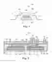
FIG. 1 illustrates a cross-sectional view of one embodiment of a module.
FIG. 2 illustrates a cross-sectional view of another embodiment of a module.
FIG. 3 illustrates a cross-sectional view of one embodiment of a connection between a bond wire and a bond pad after ball bonding.
FIG. 4 illustrates a cross-sectional view of one embodiment of a connection between the bond wire and the bond pad after annealing.
DETAILED DESCRIPTION
In the following Detailed Description, reference is made to the accompanying drawings, which form a part hereof, and in which is shown by way of illustration specific embodiments in which the invention may be practiced. In this regard, directional terminology, such as “top,” “bottom,” “front,” “back,” “leading,” “trailing,” etc., is used with reference to the orientation of the Figure(s) being described. Because components of embodiments can be positioned in a number of different orientations, the directional terminology is used for purposes of illustration and is in no way limiting. It is to be understood that other embodiments may be utilized and structural or logical changes may be made without departing from the scope of the present invention. The following detailed description, therefore, is not to be taken in a limiting sense, and the scope of the present invention is defined by the appended claims.
It is to be understood that the features of the various exemplary embodiments described herein may be combined with each other, unless specifically noted otherwise.
FIG. 1 illustrates a cross-sectional view of one embodiment of a module 100. In one embodiment, module 100 is a low power electronic module. Power electronic module 100 includes a leadframe substrate 102, a joint 104, a semiconductor chip or die 106, bond wires 108, leads 112, and a housing 110. Leadframe substrate 102 includes Cu, Al, or another suitable material. In one embodiment, leadframe substrate 102 is plated with Ni, Ag, Au, and/or Pd. In one embodiment, joint 104 is a solder joint that joins leadframe substrate 102 directly to semiconductor chip 106 using diffusion solder metals such as Cu—Sn, Au—Sn, or other suitable solders.
As used herein, the term “electrically coupled” is not meant to mean that the elements must be directly coupled together and intervening elements may be provided between the “electrically coupled” elements.
In one embodiment, leadframe substrate 102 has a thickness within the range of 125 μm to 200 μm. Leadframe substrate 102 is joined to semiconductor chip 106 via soldering or another suitable technique to provide joint 104. Housing 110 includes a mould material or another suitable material. Housing 110 surrounds leadframe substrate 102, joint 104, semiconductor chip 106, bond wires 108, and portions of leads 112. Semiconductor chip 106 is electrically coupled to leads 112 through bond wires 108. Bond wires 108 include Cu, Au, or another suitable material. In one embodiment, bond wires 108 are bonded to semiconductor chip 106 and leads 112 using thermosonic or ultrasonic wire bonding. In one embodiment, bond wires 108 are Cu and are directly bonded to Cu pads on semiconductor chip 106 via ball bonding (i.e., nail head bonding).
In a ball bonding process, a combination of heat, pressure, and/or ultrasonic energy is used to make a weld at each end of a wire. A high-voltage electric charge is applied to the wire to melt the tip of the wire, which forms into a ball due to the surface tension of the molten metal. The ball quickly solidifies and the ball is pushed onto the surface of a chip, which is typically heated. Ultrasonic energy may then be applied to the ball. The combined heat, pressure, and/or ultrasonic energy form a weld between the ball and the surface of the chip.
After the ball bonding, semiconductor chip 106 and bond wires 108 are annealed to recover the interface between each Cu pad and Cu bond wire as will be described below. In this way, a stress and void free connection between the Cu bond wire and the Cu pad is provided. In addition, since additional interface layers between the Cu pad and the Cu bond wire are not used, the number of processing steps and thus the cost to fabricate power electronic module 100 is reduced compared to typical power electronic modules. In another embodiment, a similar process is used to directly bond Au bond wires to Au pads on semiconductor chip 106.
FIG. 2 illustrates a cross-sectional view of another embodiment of a module 120. In one embodiment, module 120 is a high power electronic module. Power electronic module 120 includes a metal baseplate 124, joints 126, metalized ceramic substrates 130 including metal surfaces or layers 128 and 132, joints 134, semiconductor chips 136, bond wires 138, circuit board 140, control contacts 142, power contacts 144, potting 146 and 148, and housing 150.
Ceramic substrates 130 include Al2O3, AlN, Si3N4, or other suitable material. In one embodiment, ceramic substrates 130 each have a thickness within a range of 0.2 mm to 2.0 mm. Metal layers 128 and 132 include Cu, Al, or another suitable material. In one embodiment, metal layers 128 and/or 132 are plated with Ni, Ag, Au, and/or Pd. In one embodiment, metal layers 128 and 132 each have a thickness within a range of 0.1 mm to 0.6 mm. In one embodiment, joints 126 are solder joints that join metal layers 128 directly to metal baseplate 124 using diffusion solder metals such as Cu—Sn, Au—Sn, or other suitable solders. In one embodiment, joints 134 are solder joints that join metal layers 132 directly to semiconductor chips 136 using diffusion solder metals such as Cu—Sn, Au—Sn, or other suitable solders.
Semiconductor chips 136 may also be electrically coupled to metal layers 132 through bond wires 138. Bond wires 138 include Cu, Au, or another suitable material. In one embodiment, bond wires 138 are bonded to semiconductor chips 136 and metal layers 132 using ultrasonic wire bonding. In one embodiment, bond wires 138 are Cu and are directly bonded to Cu pads on semiconductor chips 136 via ball bonding. After the ball bonding, semiconductor chips 136 and bond wires 138 are annealed to recover the interface between each Cu pad and Cu bond wire as will be described below. In this way, a stress and void free connection between the Cu bond wire and Cu pad is provided. In addition, since additional interface layers between the Cu pad and the Cu bond wire are not used, the number of processing steps and thus the cost to fabricate power electronic module 120 is reduced compared to typical power electronic modules. In another embodiment, a similar process is used to directly bond Au bond wires to Au pads on semiconductor chips 136. In one embodiment, a similar process is also used to directly bond Cu or Au bond wires to Cu or Au metal layers 132, respectively.
Metal layers 132 are electrically coupled to circuit board 140 and power contacts 144. Circuit board 140 is electrically coupled to control contacts 142. Housing 150 encloses joints 126, metallized ceramic substrates 130 including metal layers 128 and 132, joints 134, semiconductor chips 136, bond wires 138, circuit board 140, portions of control contacts 142, and portions of power contacts 144. Housing 150 includes technical plastics or another suitable material. Housing 150 is joined to metal baseplate 124. In one embodiment, a single metallized ceramic substrate 130 is used such that metal baseplate 124 is excluded and housing 150 is joined directly to the single metallized ceramic substrate 130.
Potting material 146 fills areas below circuit board 140 within housing 150 around joints 126, metallized ceramic substrates 130 including metal layers 128 and 132, joints 134, semiconductor chips 136, and bond wires 138. Potting material 148 fills the area above circuit board 150 within housing 150 around portions of control contacts 142 and portions of power contacts 144. Potting material 146 and 148 includes silicone gel or another suitable material. Potting material 146 and 148 prevents damage to power electronic module 120 by dielectrical breakdown.
FIG. 3 illustrates a cross-sectional view of one embodiment of a connection 200 between a bond wire 202 and a bond pad 206 after ball bonding. In one embodiment, bond wire 202 provides each bond wire 108 and bond pad 206 provides each bond pad on semiconductor chip 106 as previously described and illustrated with reference to FIG. 1. In another embodiment, bond wire 202 provides each bond wire 138 and bond pad 206 provides each bond pad on semiconductor chips 136 or each metal layer 132 as previously described and illustrated with reference to FIG. 2.
Prior to ball bonding bond wire 202 to bond pad 206, the semiconductor chip including bond pad 206 is attached to a leadframe or metallized ceramic substrate. In one embodiment, the bond pad 206 is cleaned to remove any contaminants and/or oxidation on the bond pad.
Next, bond wire 202 including a ball portion 204 is attached to a bond pad 206 via ultrasonic ball bonding or another suitable technique. In one embodiment as illustrated in FIG. 3, the entire area of ball 204 is bonded to bond pad 206 at an interface 208 between ball 204 and bond pad 206. In other embodiments, portions of the area of ball 204 are bonded to bond pad 206 at interface 208 while other portions of the area at interface 208 may be micro delaminated. Due to the ultrasonic impact, the grains in the area of interface 208 are refined or smaller than grains 210 in ball 204 and grains 212 in bond pad 206. While bond wire 202 is bonded to bond pad 206 without cracks and without delamination, the connection may degrade or fail during normal operation due to the grain refinement at interface 208.
In one embodiment, bond wire 202 is Cu and bond pad 206 is Cu such that at interface 208 the Cu ball directly contacts the Cu pad. In one embodiment, the Cu bond wire is ball bonded to the Cu pad in an ambient atmosphere. In another embodiment, an inert atmosphere, which includes a nitrogen atmosphere, a forming gas atmosphere, a formic acid atmosphere, or another suitable reductive atmosphere, is used to prevent oxidation of the Cu bond wire and/or Cu pad during the bonding process. In another embodiment, bond wire 202 is Au and bond pad 206 is Au such that at the interface 208 the Au ball directly contacts the Au pad.
FIG. 4 illustrates a cross-sectional view of one embodiment of a connection 220 between bond wire 202 and bond pad 206 after annealing. Bond wire 202 and bond pad 206 are annealed at a temperature between 200° C. and 400° C. for 2 to 20 hours. During annealing, the grains at interface 208 previously described and illustrated with reference to FIG. 3 recrystallize. After annealing, the interface 208 including the smaller grains as previously described and illustrated with reference to FIG. 3 is replaced by larger grains as indicated at 222 such that there is no longer a distinguishable interface within the metal between ball 204 and bond pad 206. The grains at 222 extend between ball 204 and bond pad 206. The annealing initiates interface recovery by growing the grains across the boundary between ball 204 and bond pad 206.
The annealing also simultaneously homogenizes the solder metallization on the semiconductor chip backside for diffusion solder metals such as Cu—Sn or Au—Sn used for attaching the semiconductor chip to a leadframe or metallized ceramic substrate. For example, the annealing may homogenize the solder joint 104 previously described and illustrated with reference to FIG. 1 or the solder joints 134 and/or solder joints 126 previously described and illustrated with reference to FIG. 2. In one embodiment, the annealing is carried out using a batch process where a plurality of devices are annealed simultaneously in a suitable furnace.
Embodiments provide power electronic modules or other suitable devices including Cu or Au bond wires directly bonded to Cu or Au bond pads, respectively. An annealing process recovers the interface between the ball and bond pad by curing the contact areas followed by recrystallization of the ball and bond pad such that new crystallites grow to exceed the former interface to create a new collective grain structure. The collective structure of the Cu or Au grains provides a cohesive matrix “ball-pad” without stress and without voids. In this way, an interface between the ball and bond pad is no longer distinguishable.
Although specific embodiments have been illustrated and described herein, it will be appreciated by those of ordinary skill in the art that a variety of alternate and/or equivalent implementations may be substituted for the specific embodiments shown and described without departing from the scope of the present invention. This application is intended to cover any adaptations or variations of the specific embodiments discussed herein. Therefore, it is intended that this invention be limited only by the claims and the equivalents thereof.
Claims
What is claimed is:1. An integrated circuit comprising:
a chip comprising a copper bond pad metallization; and
a copper bond wire comprising a copper ball, the copper ball bonded directly to the copper bond pad.
2. The integrated circuit of claim 1, wherein copper grains extend between the copper bond pad and the copper ball, and
wherein the copper bond pad and the copper ball are free from an interface.
3. The integrated circuit of claim 1, further comprising:
a leadframe,
wherein the chip is attached to the leadframe, and
wherein the copper bond wire is ball bonded to the leadframe.
4. The integrated circuit of claim 1, further comprising:
a metallized ceramic substrate,
wherein the chip is attached to the metallized ceramic substrate, and
wherein the copper bond wire is ball bonded to the metallized ceramic substrate.
5. The integrated circuit of claim 4, wherein the metallized substrate comprises a copper layer, and
wherein the copper bond wire is ball bonded directly to the copper layer.
6. The integrated circuit of claim 1, wherein the chip comprises a power semiconductor component.
7. The integrated circuit of claim 6, wherein the power semiconductor component comprises one of an insulated gate bipolar transistor (IGBT) and a metal-oxide-semiconductor field effect transistor (MOSFET).
8. An integrated circuit comprising:
a chip comprising a gold bond pad; and
a gold bond wire comprising a gold ball, the gold ball bonded directly to the gold bond pad.
9. The integrated circuit of claim 8, wherein gold grains extend between the gold bond pad and the gold ball, and
wherein the gold bond pad and the gold ball are free from an interface.
10. The integrated circuit of claim 8, further comprising:
a leadframe,
wherein the chip is attached to the leadframe, and
wherein the gold bond wire is ball bonded to the leadframe.
11. The integrated circuit of claim 8, further comprising:
a metallized ceramic substrate,
wherein the chip is attached to the metallized ceramic substrate, and
wherein the gold bond wire is ball bonded to the metallized ceramic substrate.
12. A power module comprising:
a substrate;
a semiconductor chip attached to the substrate, the semiconductor chip comprising a copper bond pad; and
a copper bond wire comprising a copper ball, the copper ball bonded directly to the copper bond pad.
13. The power module of claim 12, wherein copper grains extend between the copper bond pad and the copper ball, and
wherein the copper bond pad and the copper ball are free from an interface.
14. The power module of claim 12, wherein the substrate comprises a metallized ceramic substrate.
15. The power module of claim 12, wherein the substrate comprises a leadframe.
16. The power module of claim 12, wherein the semiconductor chip comprises a power semiconductor component.
17. The power module of claim 16, wherein the power semiconductor component comprises one of an insulated gate bipolar transistor (IGBT) and a metal-oxide-semiconductor field effect transistor (MOSFET).
18. A method for fabricating an integrated circuit, the method comprising:
providing a chip comprising a copper bond pad;
attaching a copper bond wire directly to the copper bond pad; and
annealing the copper bond pad and the copper bond wire to recrystallize copper grains at a contact area between the copper bond pad and the copper bond wire such that after annealing the copper bond pad and the copper bond wire are free from an interface.
19. The method of claim 18, wherein attaching the copper bond wire to the copper bond pad comprises ultrasonic ball bonding the copper bond wire to the copper bond pad.
20. The method of claim 18, wherein attaching the copper bond wire to the copper bond pad comprises attaching the copper bond wire to the copper bond pad in an ambient atmosphere.
21. The method of claim 18, wherein attaching the copper bond wire to the copper bond pad comprises attaching the copper bond wire to the copper bond pad in an inert nitrogen atmosphere.
22. The method of claim 18, wherein attaching the copper bond wire to the copper bond pad comprises attaching the copper bond wire to the copper bond pad in one of a reductive forming gas atmosphere and a formic acid atmosphere.
23. The method of claim 18, wherein attaching the copper bond wire to the copper bond pad comprises attaching the copper bond wire to the copper bond pad in one of a nitrogen atmosphere and a forming gas atmosphere.
24. The method of claim 18, wherein annealing the copper bond pad and the copper bond wire comprises annealing at a temperature between 200° C. and 400° C.
25. The method of claim 18, wherein annealing the copper bond pad and the copper bond wire comprises annealing for a period between 2 hours and 20 hours.
Images & Drawings included:


Sources:
- United States Patent and Trademark Office - verify current appl. status at the USPTO↗
Recent applications in this class:
- » 20250285934 2025-09-11
THERMALLY-CONDUCTIVE CRYSTALLINE PEDESTAL FOR SEMICONDUCTOR DEVICE PACKAGES - » 20250279332 2025-09-04
FREQUENCY-SELECTIVE HEAT DISSIPATING DEVICE AND THIN FILM - » 20250279331 2025-09-04
HEAT DISSIPATION STRUCTURE FOR HEATING ELEMENT AND HOUSING STRUCTURE FOR BRAKE SYSTEM HAVING THE SAME - » 20250273532 2025-08-28
Interposer for Thermally Engineered Electro-Optical Multichip Modules - » 20250266318 2025-08-21
3DIC WITH HEAT DISSIPATION STRUCTURE AND WARPAGE CONTROL - » 20250259909 2025-08-14
A HEAT DISSIPATION SUBSTRATE FOR A POWER SEMICONDUCTOR MODULE, A POWER SEMICONDUCTOR MODULE INCLUDING THE SAME AND A POWER CONVERTER INCLUDING THE SAME, AND MANUFACTURING METHOD OF THE HEAT DISSIPATION SUBSTRATE FOR A POWER SEMICONDUCTOR MODULE - » 20250259908 2025-08-14
HEAT DISSIPATION SUBSTRATE FOR A POWER SEMICONDUCTOR MODULE, A POWER SEMICONDUCTOR MODULE INCLUDING THE SAME AND A POWER CONVERTER INCLUDING THE SAME, AND MANUFACTURING METHOD OF THE HEAT DISSIPATION SUBSTRATE FOR A POWER SEMICONDUCTOR MODULE - » 20250259907 2025-08-14
DISTINGUISHED FLIP CHIP PACKAGING FOR STRESS RELAXATION AND ENHANCED EM PROTECTION - » 20250253203 2025-08-07
METAL CERAMIC SUBSTRATE AND METHOD FOR PRODUCING THE SAME - » 20250246510 2025-07-31
COOLING STRUCTURE FOR A SEMICONDUCTOR DEVICE
Recent applications for this Assignee:
- » 20250293127 2025-09-18
LEADFRAME PANEL, A SEMICONDUCTOR PACKAGE COMPRISING A LEADFRAME WITH A TWO-LEVEL DAMBAR DESIGN AND A METHOD FOR FABRICATING THE SAME - » 20250285937 2025-09-11
HOUSING, SEMICONDUCTOR MODULE COMPRISING A HOUSING, AND METHOD FOR ASSEMBLING A SEMICONDUCTOR MODULE - » 20250279324 2025-09-04
PACKAGE WITH CARRIER HAVING COMPONENT ACCOMMODATION VOLUME ON ONE SIDE AND REPELLING STRUCTURE ON OTHER SIDE - » 20250266310 2025-08-21
ENCAPSULANT WITH LOW CTE AND LOW YOUNG MODULUS FOR LOW-STRESS ELECTRONIC PACKAGE - » 20250258195 2025-08-14
TEST PIN WITH POGO PIN AND SURROUNDING COIL SPRING FOR TESTING DEVICES UNDER TEST - » 20250257469 2025-08-14
METAL COMPONENT INCLUDING AN INTERMETALLIC COMPOUND LAYER AND METHOD FOR MANUFACTURING THEREOF - » 20250253195 2025-08-07
HOUSING FOR A SEMICONDUCTOR MODULE, SEMICONDUCTOR MODULE COMPRISING A HOUSING, AND METHOD FOR ASSEMBLING A SEMICONDUCTOR MODULE COMPRISING A HOUSING - » 20250240890 2025-07-24
METHOD OF EMBEDDING AN EMBEDDABLE OBJECT INTO A STACKED SUBSTRATE AND STACKED SUBSTRATE ARRANGEMENT - » 20250226297 2025-07-10
PACKAGE WITH CARRIER HAVING PLATED BOTTOM SURFACE AND SIDEWALL - » 20250219841 2025-07-03
SECURE COMMUNICATIONS USING PRE-SHARED KEYS AND LIVE MEMBERSHIP