Micromechanical method and corresponding assembly for bonding semiconductor substrates and correspondingly bonded semiconductor chip
US20120280409A1
2012-11-08
13/509,163
2010-09-23
✅ Patent granted
US 8,638,000 B2
2014-01-28
WO; PCT/EP2010/064009; 20100923
WO; WO2011/057850; 20110519
Jasmine Clark
Maginot, Moore & Beck
2030-09-23
Abstract:
A micromechanical assembly for bonding semiconductor substrates includes a semiconductor substrate having a chip pattern having a plurality of semiconductor chips, each having a functional region and an edge region surrounding the functional region. There is a bonding frame made of a bonding alloy made from at least two alloy components in the edge region, spaced apart from the functional region. Within the part of the edge region surrounding the bonding frame between the bonding frame and the functional region, there is at least one stop frame made of at least one of the alloy components, which is configured such that when a melt of the bond alloy contacts the stop frame during bonding, the bonding alloy solidifies.
Assignee:
- Robert Bosch GMBH 19,123 🇩🇪 Stuttgart, Germany
Applicant:
Interested in similar patents?
Get notified when new applications in this technology area are published.
Classification:
H01L23/48 IPC
Details of semiconductor or other solid state devices Arrangements for conducting electric current to or from the solid state body in operation, e.g. leads, terminal arrangements ; Selection of materials therefor
H01L2924/01013 » CPC further
Indexing scheme for arrangements or methods for connecting or disconnecting semiconductor or solid-state bodies as covered by; Chemical elements Aluminum [Al]
H01L2924/0132 » CPC further
Indexing scheme for arrangements or methods for connecting or disconnecting semiconductor or solid-state bodies as covered by; Alloys Binary Alloys
H01L2924/01049 » CPC further
Indexing scheme for arrangements or methods for connecting or disconnecting semiconductor or solid-state bodies as covered by; Chemical elements Indium [In]
H01L2924/01029 » CPC further
Indexing scheme for arrangements or methods for connecting or disconnecting semiconductor or solid-state bodies as covered by; Chemical elements Copper [Cu]
H01L2924/01014 » CPC further
Indexing scheme for arrangements or methods for connecting or disconnecting semiconductor or solid-state bodies as covered by; Chemical elements Silicon [Si]
H01L2924/01032 » CPC further
Indexing scheme for arrangements or methods for connecting or disconnecting semiconductor or solid-state bodies as covered by; Chemical elements Germanium [Ge]
B81C1/00269 » CPC main
Manufacture or treatment of devices or systems in or on a substrate for manufacturing microsystems; Processes for packaging MEMS devices Bonding of solid lids or wafers to the substrate
H01L23/10 » CPC further
Details of semiconductor or other solid state devices; Containers; Seals characterised by the material or arrangement of seals between parts, e.g. between cap and base of the container or between leads and walls of the container
H01L24/29 » CPC further
Arrangements for connecting or disconnecting semiconductor or solid-state bodies; Methods or apparatus related thereto; Means for bonding being attached to, or being formed on, the surface to be connected, e.g. chip-to-package, die-attach, "first-level" interconnects; Manufacturing methods related thereto; Layer connectors, e.g. plate connectors, solder or adhesive layers; Manufacturing methods related thereto; Structure, shape, material or disposition of the layer connectors prior to the connecting process of an individual layer connector
H01L24/30 » CPC further
Arrangements for connecting or disconnecting semiconductor or solid-state bodies; Methods or apparatus related thereto; Means for bonding being attached to, or being formed on, the surface to be connected, e.g. chip-to-package, die-attach, "first-level" interconnects; Manufacturing methods related thereto; Layer connectors, e.g. plate connectors, solder or adhesive layers; Manufacturing methods related thereto; Structure, shape, material or disposition of the layer connectors prior to the connecting process of a plurality of layer connectors
H01L24/32 » CPC further
Arrangements for connecting or disconnecting semiconductor or solid-state bodies; Methods or apparatus related thereto; Means for bonding being attached to, or being formed on, the surface to be connected, e.g. chip-to-package, die-attach, "first-level" interconnects; Manufacturing methods related thereto; Layer connectors, e.g. plate connectors, solder or adhesive layers; Manufacturing methods related thereto; Structure, shape, material or disposition of the layer connectors after the connecting process of an individual layer connector
H01L24/83 » CPC further
Arrangements for connecting or disconnecting semiconductor or solid-state bodies; Methods or apparatus related thereto; Methods for connecting semiconductor or other solid state bodies using means for bonding being attached to, or being formed on, the surface to be connected using a layer connector
H01L25/50 » CPC further
Assemblies consisting of a plurality of individual semiconductor or other solid state devices ; Multistep manufacturing processes thereof Multistep manufacturing processes of assemblies consisting of devices, each device being of a type provided for in group or
B81C2201/019 » CPC further
Manufacture or treatment of microstructural devices or systems in or on a substrate for making multi-layered devices, film deposition or growing Bonding or gluing multiple substrate layers
B81C2203/0118 » CPC further
Forming microstructural systems; Packaging MEMS Bonding a wafer on the substrate, i.e. where the cap consists of another wafer
B81C2203/019 » CPC further
Forming microstructural systems; Packaging MEMS; Seals characterised by the material or arrangement of seals between parts
B81C2203/036 » CPC further
Forming microstructural systems; Bonding two components; Thermal bonding Fusion bonding
H01L2224/26145 » CPC further
Indexing scheme for arrangements for connecting or disconnecting semiconductor or solid-state bodies and methods related thereto as covered by; Means for bonding being attached to, or being formed on, the surface to be connected, e.g. chip-to-package, die-attach, "first-level" interconnects; Manufacturing methods related thereto; Layer connectors, e.g. plate connectors, solder or adhesive layers; Manufacturing methods related thereto; Auxiliary members for layer connectors, e.g. spacers being formed on the semiconductor or solid-state body to be connected Flow barriers
H01L2224/30051 » CPC further
Indexing scheme for arrangements for connecting or disconnecting semiconductor or solid-state bodies and methods related thereto as covered by; Means for bonding being attached to, or being formed on, the surface to be connected, e.g. chip-to-package, die-attach, "first-level" interconnects; Manufacturing methods related thereto; Layer connectors, e.g. plate connectors, solder or adhesive layers; Manufacturing methods related thereto; Structure, shape, material or disposition of the layer connectors prior to the connecting process of a plurality of layer connectors; Shape Layer connectors having different shapes
H01L2224/30505 » CPC further
Indexing scheme for arrangements for connecting or disconnecting semiconductor or solid-state bodies and methods related thereto as covered by; Means for bonding being attached to, or being formed on, the surface to be connected, e.g. chip-to-package, die-attach, "first-level" interconnects; Manufacturing methods related thereto; Layer connectors, e.g. plate connectors, solder or adhesive layers; Manufacturing methods related thereto; Structure, shape, material or disposition of the layer connectors prior to the connecting process of a plurality of layer connectors; Material Layer connectors having different materials
H01L2224/30515 » CPC further
Indexing scheme for arrangements for connecting or disconnecting semiconductor or solid-state bodies and methods related thereto as covered by; Means for bonding being attached to, or being formed on, the surface to be connected, e.g. chip-to-package, die-attach, "first-level" interconnects; Manufacturing methods related thereto; Layer connectors, e.g. plate connectors, solder or adhesive layers; Manufacturing methods related thereto; Structure, shape, material or disposition of the layer connectors prior to the connecting process of a plurality of layer connectors; Function Layer connectors having different functions
H01L2224/32501 » CPC further
Indexing scheme for arrangements for connecting or disconnecting semiconductor or solid-state bodies and methods related thereto as covered by; Means for bonding being attached to, or being formed on, the surface to be connected, e.g. chip-to-package, die-attach, "first-level" interconnects; Manufacturing methods related thereto; Layer connectors, e.g. plate connectors, solder or adhesive layers; Manufacturing methods related thereto; Structure, shape, material or disposition of the layer connectors after the connecting process of an individual layer connector; Material at the bonding interface
H01L2224/83007 » CPC further
Indexing scheme for arrangements for connecting or disconnecting semiconductor or solid-state bodies and methods related thereto as covered by; Methods for connecting semiconductor or other solid state bodies using means for bonding being attached to, or being formed on, the surface to be connected using a layer connector involving a permanent auxiliary member being left in the finished device, e.g. aids for holding or protecting the layer connector during or after the bonding process
H01L2224/83095 » CPC further
Indexing scheme for arrangements for connecting or disconnecting semiconductor or solid-state bodies and methods related thereto as covered by; Methods for connecting semiconductor or other solid state bodies using means for bonding being attached to, or being formed on, the surface to be connected using a layer connector; Bonding environment Temperature settings
H01L2224/83191 » CPC further
Indexing scheme for arrangements for connecting or disconnecting semiconductor or solid-state bodies and methods related thereto as covered by; Methods for connecting semiconductor or other solid state bodies using means for bonding being attached to, or being formed on, the surface to be connected using a layer connector; Arrangement of the layer connectors prior to mounting wherein the layer connectors are disposed only on the semiconductor or solid-state body
H01L2224/83365 » CPC further
Indexing scheme for arrangements for connecting or disconnecting semiconductor or solid-state bodies and methods related thereto as covered by; Methods for connecting semiconductor or other solid state bodies using means for bonding being attached to, or being formed on, the surface to be connected using a layer connector; Bonding interfaces of the semiconductor or solid state body Shape, e.g. interlocking features
H01L2224/83815 » CPC further
Indexing scheme for arrangements for connecting or disconnecting semiconductor or solid-state bodies and methods related thereto as covered by; Methods for connecting semiconductor or other solid state bodies using means for bonding being attached to, or being formed on, the surface to be connected using a layer connector; Bonding techniques; Soldering or alloying Reflow soldering
H01L2924/01005 » CPC further
Indexing scheme for arrangements or methods for connecting or disconnecting semiconductor or solid-state bodies as covered by; Chemical elements Boron [B]
H01L2924/01006 » CPC further
Indexing scheme for arrangements or methods for connecting or disconnecting semiconductor or solid-state bodies as covered by; Chemical elements Carbon [C]
H01L2924/01033 » CPC further
Indexing scheme for arrangements or methods for connecting or disconnecting semiconductor or solid-state bodies as covered by; Chemical elements Arsenic [As]
H01L2924/01082 » CPC further
Indexing scheme for arrangements or methods for connecting or disconnecting semiconductor or solid-state bodies as covered by; Chemical elements Lead [Pb]
H01L2924/01322 » CPC further
Indexing scheme for arrangements or methods for connecting or disconnecting semiconductor or solid-state bodies as covered by; Alloys; Binary Alloys Eutectic Alloys, i.e. obtained by a liquid transforming into two solid phases
H01L2924/1631 » CPC further
Indexing scheme for arrangements or methods for connecting or disconnecting semiconductor or solid-state bodies as covered by; Details of package parts other than the semiconductor or other solid state devices to be connected; Cap; Connection portion, e.g. seal Structure
H01L2924/165 » CPC further
Indexing scheme for arrangements or methods for connecting or disconnecting semiconductor or solid-state bodies as covered by; Details of package parts other than the semiconductor or other solid state devices to be connected; Cap; Connection portion, e.g. seal; Material with a principal constituent of the material being a metal or a metalloid, e.g. boron [B], silicon [Si], germanium [Ge], arsenic [As], antimony [Sb], tellurium [Te] and polonium [Po], and alloys thereof
H01L2924/014 » CPC further
Indexing scheme for arrangements or methods for connecting or disconnecting semiconductor or solid-state bodies as covered by; Alloys Solder alloys
H01L2924/01079 » CPC further
Indexing scheme for arrangements or methods for connecting or disconnecting semiconductor or solid-state bodies as covered by; Chemical elements Gold [Au]
H01L2924/0105 » CPC further
Indexing scheme for arrangements or methods for connecting or disconnecting semiconductor or solid-state bodies as covered by; Chemical elements Tin [Sn]
H01L2924/00014 » CPC further
Indexing scheme for arrangements or methods for connecting or disconnecting semiconductor or solid-state bodies as covered by; Technical content checked by a classifier the subject-matter covered by the group, the symbol of which is combined with the symbol of this group, being disclosed without further technical details
H01L2924/1461 » CPC further
Indexing scheme for arrangements or methods for connecting or disconnecting semiconductor or solid-state bodies as covered by; Details of semiconductor or other solid state devices to be connected; Mixed devices MEMS
H01L2924/00 » CPC further
Indexing scheme for arrangements or methods for connecting or disconnecting semiconductor or solid-state bodies as covered by
H01L21/30 IPC
Processes or apparatus adapted for the manufacture or treatment of semiconductor or solid state devices or of parts thereof; Manufacture or treatment of semiconductor devices or of parts thereof the devices having at least one potential-jump barrier or surface barrier, e.g. PN junction, depletion layer or carrier concentration layer the devices having semiconductor bodies comprising elements of Group IV of the Periodic System or AB compounds with or without impurities, e.g. doping materials Treatment of semiconductor bodies using processes or apparatus not provided for in groups -
Description
PRIOR ART
The present invention relates to a micromechanical method and a corresponding assembly for bonding semiconductor substrates and a corresponding bonded semiconductor chip.
Although applicable to any micromechanical components and structures, in particular sensors and actuators, the present invention and the problem area addressed thereby will be explained with regard to a micromechanical sensor that can be produced using the technology of silicon surface micromachining.
Micromechanical substrate connections, e.g. wafer-wafer bonding connections, are usually realized by eutectic alloys comprising two or more solid bonding materials or alloy components as constituents. Eutectic alloys of this type have an unambiguously determinable melting point. By contrast, other mixing ratios with the same alloy components have a melting or solidification range in which, alongside the melt, a solid phase is also present. The melting point of the eutectic alloy is, moreover, the lowest of all mixtures composed of the same constituents.
During the bonding process, a minimum required bonding force has to be applied in order to bring the bonding alloys into contact at the wafer level. This causes the liquid eutectic phase to flow. In this case, it can happen that the liquid eutectic phase flows into MEMS functional regions in an uncontrolled manner. In order to minimize or prevent such flowing, it is possible to provide, for example, a very wide stop trench in each case on the inside and outside around the bonding frame, as a result of which an increased area requirement at the chip level has to be kept available.
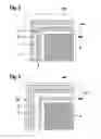
FIG. 5 is a schematic partial plan view of a chip region of an exemplary assembly for bonding semiconductor substrates.
The micromechanical sensor chip 1, which has an active functional region 4 and a passive edge region 4a. Provided in the edge region 4a is a bonding frame 2 with an applied eutectic bonding alloy, for example Al—Ge, which divides the edge region 4a into an inner region 4a2, which is surrounded by the bonding frame, and an outer region 4a1. A stop trench 3 lies in the inner region 4a2 between bonding frame 2 and functional region 4 of the sensor chip 1, said stop trench being intended to prevent melt from flowing from the region of the bonding frame 2 into the functional region 4 during the bonding process. The part of the melt flowing during the bonding process is therefore intercepted by the use of the stop trench 3. Typical dimensions of such a stop trench 3 are between 20 and 50 μm in terms of the width b. Said stop trench 3 additionally requires both a minimum distance d1 with respect to the bonding frame 2 and a minimum distance d2 with respect to the active functional region 4. As a result, an inconsiderable area requirement is necessary precisely in the case of sensor chips that are becoming ever smaller.
WO 2005/008772 A2 discloses an electronic component comprising a semiconductor chip and a lead frame having a metal coating pattern on its underside for the soldering of the electronic component. Said metal coating pattern has wetting regions, which can be wetted with solder material, and anti-wetting regions, which cannot be wetted with solder material, wherein the electronic component has solder deposits on the wetting regions on the underside.
ADVANTAGES OF THE INVENTION
The assembly according to the invention according to claim 1 and the micromechanical method for bonding semiconductor substrates according to claim 8 and the corresponding bonded semiconductor chip according to claim 9 have the advantage that, as a result of the introduction of a comparatively small structured stop frame composed of at least one of the alloy components, at least within and preferably within and outside the actual bonding frame, the flowing melt is stopped.
The stop frame composed of at least one of the alloy components can be embodied, independently of the lithography and patterning processes used, with a width of between 0.1 and 50 μm, preferably between 1 and 20 μm, and particularly preferably between 5 and 10 μm, and thus constitutes a significantly smaller area requirement in comparison with the stop trenches. The distance with respect to the bonding frame and with respect to the functional region of the sensor can be made significantly smaller in comparison with the stop trenches, preferably between 1 and 20 μm and particularly preferably between 5 and 10 μm.
The concept on which the present invention is based consists in providing a compensation structure composed of at least one of the alloy materials for in-situ solidification of the liquid phase. The underlying mechanism is that the melt solidifies upon contact with the additionally provided material of the alloy component since the new composition has a higher melting point, e.g. the eutectic composition, is no longer provided, and, consequently, no further flowing is possible.
Preferably, the bonding alloy consists of one of the following mixtures: Au—Si, Al—Ge, Cu—Sn, Au—In and alloys composed of the respective individual materials under consideration, such as e.g. AlSiCu—GE, AlSi—Ge or AlCu—Ge. All alloying partners that can be used in micromechanics are conceivable, in principle.
Alloying partners whose phase diagrams provide a eutectic alloy are particularly preferred. One exemplary alloy is Al—Ge. The melting points of the two bonding materials are 660° C. for pure aluminum and 938° C. for pure germanium. The melting point at the eutectic point is 420° C. During eutectic bonding, the critical bonding temperature required for bonding is dependent on the mixture of the materials used. In the ideal case, a liquid phase forms at the melting point at the eutectic point. In the exemplary case of the Al—Ge alloy, the actual bonding temperature is usually in the range of 420° C. to 450° C.
Furthermore, the stop structures according to the invention also do not result in the production of an unnecessarily high topography, such as e.g. as a result of a stop trench.
Advantageous developments and improvements of the respective subject matter of the invention are found in the dependent claims.
DRAWINGS
Exemplary embodiments of the invention are illustrated in the drawing and explained in greater detail in the following description.
In the figures:
FIG. 1a shows a schematic partial plan view of a chip region of an assembly for bonding semiconductor substrates in accordance with a first embodiment of the present invention;
FIG. 1b shows a schematic partial cross-sectional view of a bonded chip manufactured from the assembly for bonding semiconductor substrates in accordance with the first embodiment of the present invention;
FIG. 2 shows a schematic partial plan view of a chip region of an assembly for bonding semiconductor substrates in accordance with a second embodiment of the present invention;
FIG. 3 shows a schematic partial plan view of a chip region of an assembly for bonding semiconductor substrates in accordance with a third embodiment of the present invention;
FIG. 4 shows a schematic partial plan view of a chip region of an assembly for bonding semiconductor substrates in accordance with a fourth embodiment of the present invention; and
FIG. 5 shows a schematic partial plan view of a chip region of an exemplary assembly for bonding semiconductor substrates.
DESCRIPTION OF THE EXEMPLARY EMBODIMENTS
In the figures, identical reference symbols designate identical or functionally identical parts.
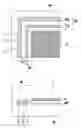
FIG. 1a is a schematic partial plan view of a chip region of an assembly for bonding semiconductor substrates in accordance with a first embodiment of the present invention.
The micromechanical sensor chip 1, which has an active functional region 4 and a passive edge region 4a. Provided in the edge region 4a is a bonding frame 2 with an applied eutectic bonding alloy, for example Al—Ge, which splits the edge region 4a into an inner region 4a2, which is surrounded by the bonding frame, and an outer region 4a1. A stop frame 7 is arranged in the inner region 4a2 between bonding frame 2 and functional region 4 of the sensor chip 1, said stop frame consisting of a non-eutectic alloy composed of Al and Ge, that is to say having either a higher Ge content or a higher Al content (up to the respective pure alloy component) than the corresponding eutectic alloy.
This additionally provided stop frame 7, upon contact with the flow movement (proceeding from the bonding frame 2) of the eutectic melt produced, leads to a change in the solubility of the bonding alloy and alters the material composition of the melt in such a way that the melt solidifies instantaneously and cannot flow further.
The stop frame 7 can be embodied, independently of the lithography and patterning processes used, with a width of between 0.1 and 50 μm, preferably between 1 and 20 μm, and particularly preferably between 5 and 10 μm, and, consequently, constitutes a significantly smaller area requirement in comparison with the stop trenches, which is designated as width b′ in FIG. 1a. The distance d1′ with respect to the bonding frame and the distance d2′ with respect to the functional region of the sensor can be made significantly smaller in comparison with the stop trenches mentioned above, preferably between 1 and 20 μm and particularly preferably between 5 and 10 μm.
FIG. 1b is a schematic partial cross-sectional view of a bonded chip manufactured from the assembly for bonding of semiconductor substrates in accordance with the first embodiment of the present invention.
The bonded semiconductor chip has a first chip half 1 having a chip in accordance with FIG. 1, and furthermore a second chip half 10, which has a bonding surface BF, onto which the bonding frame 2 is bonded. There is a region 7 of solidified bonding alloy, which runs between the bonding frame 2 and stop frame 7, in which the stop frame 7 has intercepted the melt flowing during the bonding process.
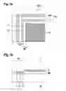
FIG. 2 is a schematic partial plan view of a chip region of an assembly for bonding semiconductor substrates in accordance with a second embodiment of the present invention.
In the case of the second embodiment in accordance with FIG. 2, a double stop frame 7a, 7b with an interspace Z situated between the two stop frames 7a, 7b is provided. In the case of this second embodiment, in addition to altering the mixing ratio of the alloy out of the eutectic range, it is possible to utilize the capillary effect that forms between the two stop frames 7a, 7b, which are led in a parallel fashion, in the interspace Z. As a result of this capillary effect, relatively large amounts of a eutectic melt which occur locally can be rapidly distributed along the stop frames 7a, 7b by way of the interspace Z. This rapid distribution provides for the supply of a substantial amount of contact with the material of the stop frames, which accelerates the solidification, in order thus to be able to prevent even more effectively an “overflow” at a location greatly exposed to eutectic melt.
Otherwise, the second embodiment corresponds to the first embodiment.
FIG. 3 is a schematic partial plan view of a chip region of an assembly for bonding semiconductor substrates in accordance with a third embodiment of the present invention.
In the case of the third embodiment in accordance with FIG. 3, a respective stop frame 7a′ and 7b′ composed of a non-eutectic alloy or one of the alloy components are provided both outside the bonding frame 2 and within the bonding frame 2.
Otherwise, the third embodiment corresponds to the first and second embodiments.
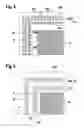
FIG. 4 is a schematic partial plan view of a chip region of an assembly for bonding semiconductor substrates in accordance with a fourth embodiment of the present invention.
In the case of the fourth embodiment in accordance with FIG. 4, examples are given of structures which can form a discontinuous stop frame, to be precise respectively by themselves or in combination with one another. The stop frame patterns comprise a point pattern 70a, a square pattern 70b, a triangle pattern 70c, a star pattern 70d and a line pattern 70e. It goes without saying that any other geometries are conceivable, where account should be taken of a width comparable to that in the case of a corresponding continuous stop frame and a distance d that is not so large, of typically 1 to 15 μm, between the individual structure elements.
Otherwise, the fourth embodiment corresponds to the first to third embodiments.
Although the present invention has been described above on the basis of preferred exemplary embodiments, it is not restricted thereto, but rather can be modified in diverse ways.
Although specific patterns and alloys have been specified in the above embodiments, the present invention is not restricted thereto, and it is possible, of course, to use patterns and alloys which deviate therefrom and which bring about the effect of the solidification of an overflowing melt.
Moreover, the invention is not restricted to eutectic mixtures, but rather can be applied to all alloys whose melting point can be increased by the addition of at least one of the alloy components.
Claims
1. An assembly for bonding semiconductor substrates comprising:
a semiconductor substrate having a chip pattern having a multiplicity of semiconductor chips each having a functional region and an edge region surrounding the functional region;
a bonding frame composed of a bonding alloy composed of at least two alloy components and provided in the edge region at a distance from the functional region; and
at least one stop frame composed of at least one of the alloy components and provided within that part of the edge region which is surrounded by the bonding frame between the bonding frame and the functional region,
wherein said at least one stop frame is configured in such a way that, when a melt of the bonding alloy impinges on the stop frame during bonding, solidification of the bonding alloy occurs.
2. The assembly as claimed in claim 1, wherein two stop frames each composed of at least one of the alloy components are provided between the bonding frame and the functional region, said stop frames running substantially parallel and forming an interspace.
3. The assembly as claimed in claim 1, wherein the bonding frame has a pattern structure composed of discrete pattern elements with a respective intermediate distance.
4. The assembly as claimed in claim 1, further comprising:
at least one further stop frame composed of at least one of the alloy components and provided in the edge region within that part of the edge region which is not surrounded by the bonding frame,
wherein said at least one further stop frame is configured in such a way that, when a melt of the bonding alloy impinges on the further stop frame during bonding, solidification of the bonding alloy occurs.
5. The assembly as claimed in claim 1, wherein the bonding alloy has a eutectic composition.
6. The assembly as claimed in claim 1, wherein the bonding alloy consists of one of the following mixtures: Au—Si, Al—Ge, Cu—Sn, Au—In and alloys composed of the respective individual materials under consideration, including AlSiCu—GE, AlSi—Ge or AlCu—Ge.
7. The assembly as claimed in claim 1, wherein the substrate is a semiconductor wafer.
8. A micromechanical method for bonding semiconductor substrates comprising:
heating an assembly above the melting point of a bonding alloy; and
bonding the heated assembly on to a further semiconductor substrate under pressure,
wherein the assembly includes (i) a semiconductor substrate having a chip pattern having a multiplicity of semiconductor chips each having a functional region and an edge region surrounding the functional region, (ii) a bonding frame composed of the bonding alloy composed of at least two alloy components and provided in the edge region at a distance from the functional region, and (iii) at least one stop frame composed of at least one of the alloy components and provided within that part of the edge region which is surrounded by the bonding frame between the bonding frame and the functional region,
wherein said at least one stop frame is configured in such a way that, when a melt of the bonding alloy impinges on the stop frame during bonding, solidification of the bonding alloy occurs, and
wherein part of the melt of the bonding alloy flows to the stop frame and solidifies there, without reaching the functional region.
9. A bonded semiconductor chip comprising:
a first chip half having a functional region and an edge region surrounding the functional region;
a bonding frame composed of a bonding alloy composed of at least two alloy components and provided in the edge region at a distance from the functional region;
at least one stop frame composed of at least one of the alloy components and provided within that part of the edge region which is surrounded by the bonding frame between the bonding frame and the functional region,
wherein said at least one stop frame is configured in such a way that, when a melt of the bonding alloy impinges on the stop frame during bonding, solidification of the bonding alloy occurs, and
wherein a second chip half, which has a bonding surface, onto which the bonding frame is bonded.
10. The bonded semiconductor chip as claimed in claim 9, wherein there is a region of solidified bonding alloy which runs between the bonding frame and stop frame.
Images & Drawings included:
Sources:
- United States Patent and Trademark Office - verify current appl. status at the USPTO↗
Recent applications in this class:
- » 20250236512 2025-07-24
BOND FORCE CONCENTRATOR - » 20250236511 2025-07-24
Inertial Sensor And Electronic Component - » 20250136438 2025-05-01
Bond force concentrator - » 20250109015 2025-04-03
MICROELECTROMECHANICAL COMPONENT WITH GAP-CONTROL STRUCTURE AND A METHOD FOR MANUFACTURING IT - » 20250011165 2025-01-09
MICRO-ELECTRO-MECHANICAL SYSTEM PACKAGE AND FABRICATION METHOD THEREOF - » 20240425364 2024-12-26
DIE STACKING WITH CONTROLLED TILT AND ANGULAR ALIGNMENT - » 20240417244 2024-12-19
ENCLOSURE - » 20240409398 2024-12-12
MEMS DEVICE WITH A CAP LAYER HAVING GAPS AND METHOD OF MANUFACTURING A MEMS DEVICE - » 20240317579 2024-09-26
MEMS SENSOR, AND METHOD FOR MANUFACTURING MEMS SENSOR - » 20240253978 2024-08-01
WIRING BOARD ASSEMBLY, LID ASSEMBLY, PACKAGE SET, AND METHOD FOR MANUFACTURING ELECTRONIC COMPONENT
Recent applications for this Assignee:
- » 20250154889 2025-05-15
PRESSURE CONTROL IN AN EXHAUST AFTERTREATMENT SYSTEM - » 20250154580 2025-05-15
ENZYME TRANSLOCATORS IN NANOGAP WITH 3' -ESTERS - » 20250147582 2025-05-08
METHOD FOR DETERMINING AN EYE DISTANCE IN A PAIR OF DATA GLASSES, AND DATA GLASSES - » 20250146568 2025-05-08
DRIVE ASSEMBLY AND VEHICLE HAVING SUCH A DRIVE ASSEMBLY - » 20250146495 2025-05-08
Flexible Pump Assembly for Use in a Fan Drive - » 20250140882 2025-05-01
FUEL CELL SYSTEM HAVING ENERGY RECUPERATION - » 20250137810 2025-05-01
METHOD FOR MATCHING A DIGITAL ROAD MAP - » 20250137033 2025-05-01
DNA UNFOLDING USING A FREE-END TAG FLOW MODIFIER - » 20250119751 2025-04-10
A BLUETOOTH COMMUNICATION METHOD AND SYSTEM - » 20250118116 2025-04-10
Diagnostic Protocol Search With Improved Efficiency