Methods of fluxless micro-piercing of solder balls, and resulting devices
US20150008577A1
2015-01-08
14/201,031
2014-03-07
✅ Patent granted
US 10,163,840 B2
2018-12-25
-
-
Mary Wilczewski
Perkins Coie LLP
2036-02-08
Abstract:
A method of establishing conductive connections is disclosed. The method includes providing an integrated circuit die having a plurality of solder balls each of which has an oxide layer on an outer surface of the solder ball. The method also includes performing a heating process to heat at least the solder balls and applying a force causing each of a plurality of piercing bond structures on a substrate to pierce one of the solder balls and its associated oxide layer to thereby establish a conductive connection between the solder ball and the piercing bond structure.
Assignee:
- Micron Technology, Inc. 27,672 🇺🇸 Boise, ID, United States
Applicant:
Interested in similar patents?
Get notified when new applications in this technology area are published.
Classification:
H01L24/14 » CPC main
Arrangements for connecting or disconnecting semiconductor or solid-state bodies; Methods or apparatus related thereto; Means for bonding being attached to, or being formed on, the surface to be connected, e.g. chip-to-package, die-attach, "first-level" interconnects; Manufacturing methods related thereto; Bump connectors ; Manufacturing methods related thereto; Structure, shape, material or disposition of the bump connectors prior to the connecting process of a plurality of bump connectors
H01L21/4846 » CPC further
Processes or apparatus adapted for the manufacture or treatment of semiconductor or solid state devices or of parts thereof; Manufacture or treatment of semiconductor devices or of parts thereof the devices having at least one potential-jump barrier or surface barrier, e.g. PN junction, depletion layer or carrier concentration layer; Manufacture or treatment of parts, e.g. containers, prior to assembly of the devices, using processes not provided for in a single one of the subgroups -; Conductive parts Leads on or in insulating or insulated substrates, e.g. metallisation
H01L23/481 » CPC further
Details of semiconductor or other solid state devices; Arrangements for conducting electric current to or from the solid state body in operation, e.g. leads, terminal arrangements ; Selection of materials therefor Internal lead connections, e.g. via connections, feedthrough structures
H01L23/49811 » CPC further
Details of semiconductor or other solid state devices; Arrangements for conducting electric current to or from the solid state body in operation, e.g. leads, terminal arrangements ; Selection of materials therefor consisting of soldered constructions; Leads, on insulating substrates, Additional leads joined to the metallisation on the insulating substrate, e.g. pins, bumps, wires, flat leads
H01L24/06 » CPC further
Arrangements for connecting or disconnecting semiconductor or solid-state bodies; Methods or apparatus related thereto; Means for bonding being attached to, or being formed on, the surface to be connected, e.g. chip-to-package, die-attach, "first-level" interconnects; Manufacturing methods related thereto; Bonding areas ; Manufacturing methods related thereto; Structure, shape, material or disposition of the bonding areas prior to the connecting process of a plurality of bonding areas
H01L24/17 » CPC further
Arrangements for connecting or disconnecting semiconductor or solid-state bodies; Methods or apparatus related thereto; Means for bonding being attached to, or being formed on, the surface to be connected, e.g. chip-to-package, die-attach, "first-level" interconnects; Manufacturing methods related thereto; Bump connectors ; Manufacturing methods related thereto; Structure, shape, material or disposition of the bump connectors after the connecting process of a plurality of bump connectors
H01L24/81 » CPC further
Arrangements for connecting or disconnecting semiconductor or solid-state bodies; Methods or apparatus related thereto; Methods for connecting semiconductor or other solid state bodies using means for bonding being attached to, or being formed on, the surface to be connected using a bump connector
H05K3/325 » CPC further
Apparatus or processes for manufacturing printed circuits; Assembling printed circuits with electric components, e.g. with resistor electrically connecting electric components or wires to printed circuits by abutting or pinching, i.e. without alloying process; mechanical auxiliary parts therefor
H05K3/4007 » CPC further
Apparatus or processes for manufacturing printed circuits; Forming printed elements for providing electric connections to or between printed circuits Surface contacts, e.g. bumps
H05K3/4007 » CPC further
Apparatus or processes for manufacturing printed circuits; Forming printed elements for providing electric connections to or between printed circuits Surface contacts, e.g. bumps
H01L24/13 » CPC further
Arrangements for connecting or disconnecting semiconductor or solid-state bodies; Methods or apparatus related thereto; Means for bonding being attached to, or being formed on, the surface to be connected, e.g. chip-to-package, die-attach, "first-level" interconnects; Manufacturing methods related thereto; Bump connectors ; Manufacturing methods related thereto; Structure, shape, material or disposition of the bump connectors prior to the connecting process of an individual bump connector
H01L24/16 » CPC further
Arrangements for connecting or disconnecting semiconductor or solid-state bodies; Methods or apparatus related thereto; Means for bonding being attached to, or being formed on, the surface to be connected, e.g. chip-to-package, die-attach, "first-level" interconnects; Manufacturing methods related thereto; Bump connectors ; Manufacturing methods related thereto; Structure, shape, material or disposition of the bump connectors after the connecting process of an individual bump connector
H01L2224/0401 » CPC further
Indexing scheme for arrangements for connecting or disconnecting semiconductor or solid-state bodies and methods related thereto as covered by; Means for bonding being attached to, or being formed on, the surface to be connected, e.g. chip-to-package, die-attach, "first-level" interconnects; Manufacturing methods related thereto; Bonding areas; Manufacturing methods related thereto; Structure, shape, material or disposition of the bonding areas prior to the connecting process Bonding areas specifically adapted for bump connectors, e.g. under bump metallisation [UBM]
H01L2224/0603 » CPC further
Indexing scheme for arrangements for connecting or disconnecting semiconductor or solid-state bodies and methods related thereto as covered by; Means for bonding being attached to, or being formed on, the surface to be connected, e.g. chip-to-package, die-attach, "first-level" interconnects; Manufacturing methods related thereto; Bonding areas; Manufacturing methods related thereto; Structure, shape, material or disposition of the bonding areas prior to the connecting process of a plurality of bonding areas; Structure Bonding areas having different sizes, e.g. different heights or widths
H01L2224/1012 » CPC further
Indexing scheme for arrangements for connecting or disconnecting semiconductor or solid-state bodies and methods related thereto as covered by; Means for bonding being attached to, or being formed on, the surface to be connected, e.g. chip-to-package, die-attach, "first-level" interconnects; Manufacturing methods related thereto; Bump connectors; Manufacturing methods related thereto Auxiliary members for bump connectors, e.g. spacers
H01L2224/1403 » CPC further
Indexing scheme for arrangements for connecting or disconnecting semiconductor or solid-state bodies and methods related thereto as covered by; Means for bonding being attached to, or being formed on, the surface to be connected, e.g. chip-to-package, die-attach, "first-level" interconnects; Manufacturing methods related thereto; Bump connectors; Manufacturing methods related thereto; Structure, shape, material or disposition of the bump connectors prior to the connecting process of a plurality of bump connectors; Structure Bump connectors having different sizes, e.g. different diameters, heights or widths
H01L2224/73103 » CPC further
Indexing scheme for arrangements for connecting or disconnecting semiconductor or solid-state bodies and methods related thereto as covered by; Means for bonding being of different types provided for in two or more of groups; Location prior to the connecting process on the same surface Bump and layer connectors
H01L2224/73204 » CPC further
Indexing scheme for arrangements for connecting or disconnecting semiconductor or solid-state bodies and methods related thereto as covered by; Means for bonding being of different types provided for in two or more of groups; Location after the connecting process on the same surface; Bump and layer connectors the bump connector being embedded into the layer connector
H01L2224/812 » CPC further
Indexing scheme for arrangements for connecting or disconnecting semiconductor or solid-state bodies and methods related thereto as covered by; Methods for connecting semiconductor or other solid state bodies using means for bonding being attached to, or being formed on, the surface to be connected using a bump connector Applying energy for connecting
H01L2224/8114 » CPC further
Indexing scheme for arrangements for connecting or disconnecting semiconductor or solid-state bodies and methods related thereto as covered by; Methods for connecting semiconductor or other solid state bodies using means for bonding being attached to, or being formed on, the surface to be connected using a bump connector; Aligning involving guiding structures, e.g. spacers or supporting members the guiding structures being at least partially left in the finished device Guiding structures outside the body
H01L2224/81136 » CPC further
Indexing scheme for arrangements for connecting or disconnecting semiconductor or solid-state bodies and methods related thereto as covered by; Methods for connecting semiconductor or other solid state bodies using means for bonding being attached to, or being formed on, the surface to be connected using a bump connector; Aligning involving guiding structures, e.g. spacers or supporting members
H01L2224/81138 » CPC further
Indexing scheme for arrangements for connecting or disconnecting semiconductor or solid-state bodies and methods related thereto as covered by; Methods for connecting semiconductor or other solid state bodies using means for bonding being attached to, or being formed on, the surface to be connected using a bump connector; Aligning involving guiding structures, e.g. spacers or supporting members the guiding structures being at least partially left in the finished device
H01L2224/81193 » CPC further
Indexing scheme for arrangements for connecting or disconnecting semiconductor or solid-state bodies and methods related thereto as covered by; Methods for connecting semiconductor or other solid state bodies using means for bonding being attached to, or being formed on, the surface to be connected using a bump connector; Arrangement of the bump connectors prior to mounting wherein the bump connectors are disposed on both the semiconductor or solid-state body and another item or body to be connected to the semiconductor or solid-state body
H01L2224/81208 » CPC further
Indexing scheme for arrangements for connecting or disconnecting semiconductor or solid-state bodies and methods related thereto as covered by; Methods for connecting semiconductor or other solid state bodies using means for bonding being attached to, or being formed on, the surface to be connected using a bump connector; Applying energy for connecting; Compression bonding applying unidirectional static pressure
H01L2224/81801 » CPC further
Indexing scheme for arrangements for connecting or disconnecting semiconductor or solid-state bodies and methods related thereto as covered by; Methods for connecting semiconductor or other solid state bodies using means for bonding being attached to, or being formed on, the surface to be connected using a bump connector; Bonding techniques Soldering or alloying
H01L2224/83192 » CPC further
Indexing scheme for arrangements for connecting or disconnecting semiconductor or solid-state bodies and methods related thereto as covered by; Methods for connecting semiconductor or other solid state bodies using means for bonding being attached to, or being formed on, the surface to be connected using a layer connector; Arrangement of the layer connectors prior to mounting wherein the layer connectors are disposed only on another item or body to be connected to the semiconductor or solid-state body
H01L2224/83194 » CPC further
Indexing scheme for arrangements for connecting or disconnecting semiconductor or solid-state bodies and methods related thereto as covered by; Methods for connecting semiconductor or other solid state bodies using means for bonding being attached to, or being formed on, the surface to be connected using a layer connector; Arrangement of the layer connectors prior to mounting Lateral distribution of the layer connectors
H01L2924/014 » CPC further
Indexing scheme for arrangements or methods for connecting or disconnecting semiconductor or solid-state bodies as covered by; Alloys Solder alloys
H01L2924/0105 » CPC further
Indexing scheme for arrangements or methods for connecting or disconnecting semiconductor or solid-state bodies as covered by; Chemical elements Tin [Sn]
H01L2924/01005 » CPC further
Indexing scheme for arrangements or methods for connecting or disconnecting semiconductor or solid-state bodies as covered by; Chemical elements Boron [B]
H01L2924/01006 » CPC further
Indexing scheme for arrangements or methods for connecting or disconnecting semiconductor or solid-state bodies as covered by; Chemical elements Carbon [C]
H01L2924/01028 » CPC further
Indexing scheme for arrangements or methods for connecting or disconnecting semiconductor or solid-state bodies as covered by; Chemical elements Nickel [Ni]
H01L2924/01033 » CPC further
Indexing scheme for arrangements or methods for connecting or disconnecting semiconductor or solid-state bodies as covered by; Chemical elements Arsenic [As]
H01L2924/01051 » CPC further
Indexing scheme for arrangements or methods for connecting or disconnecting semiconductor or solid-state bodies as covered by; Chemical elements Antimony [Sb]
H01L2924/01078 » CPC further
Indexing scheme for arrangements or methods for connecting or disconnecting semiconductor or solid-state bodies as covered by; Chemical elements Platinum [Pt]
H01L2924/01079 » CPC further
Indexing scheme for arrangements or methods for connecting or disconnecting semiconductor or solid-state bodies as covered by; Chemical elements Gold [Au]
H01L2924/01082 » CPC further
Indexing scheme for arrangements or methods for connecting or disconnecting semiconductor or solid-state bodies as covered by; Chemical elements Lead [Pb]
H01L2924/14 » CPC further
Indexing scheme for arrangements or methods for connecting or disconnecting semiconductor or solid-state bodies as covered by; Details of semiconductor or other solid state devices to be connected; Device type Integrated circuits
H01L2924/15311 » CPC further
Indexing scheme for arrangements or methods for connecting or disconnecting semiconductor or solid-state bodies as covered by; Details of package parts other than the semiconductor or other solid state devices to be connected; Die mounting substrate; Connection portion the connection portion being formed only on the surface of the substrate opposite to the die mounting surface being a ball array, e.g. BGA
H01L2924/20105 » CPC further
Indexing scheme for arrangements or methods for connecting or disconnecting semiconductor or solid-state bodies as covered by; Parameters; Temperature ranges Temperature range 150 C=
H01L2924/20106 » CPC further
Indexing scheme for arrangements or methods for connecting or disconnecting semiconductor or solid-state bodies as covered by; Parameters; Temperature ranges Temperature range 200 C=
H05K3/06 » CPC further
Apparatus or processes for manufacturing printed circuits in which the conductive material is applied to the surface of the insulating support and is thereafter removed from such areas of the surface which are not intended for current conducting or shielding the conductive material being removed chemically or electrolytically, e.g. by photo-etch process
H05K2201/0367 » CPC further
Indexing scheme relating to printed circuits covered by; Conductive materials; Structure of the conductor; Conductor shape Metallic bump or raised conductor not used as solder bump
H05K2201/0367 » CPC further
Indexing scheme relating to printed circuits covered by; Conductive materials; Structure of the conductor; Conductor shape Metallic bump or raised conductor not used as solder bump
H05K2201/10674 » CPC further
Indexing scheme relating to printed circuits covered by; Details of components or other objects attached to or integrated in a printed circuit board; Details of electrical connections of non-printed components, e.g. special leads; Components characterised by their electrical contacts Flip chip
H05K2201/10734 » CPC further
Indexing scheme relating to printed circuits covered by; Details of components or other objects attached to or integrated in a printed circuit board; Details of electrical connections of non-printed components, e.g. special leads; Components characterised by their electrical contacts Ball grid array [BGA]; Bump grid array
H05K2201/10977 » CPC further
Indexing scheme relating to printed circuits covered by; Details of components or other objects attached to or integrated in a printed circuit board; Details of electrical connections of non-printed components, e.g. special leads; Other details of electrical connections Encapsulated connections
H05K2203/0315 » CPC further
Indexing scheme relating to apparatus or processes for manufacturing printed circuits covered by; Metal processing Oxidising metal
H05K2203/0315 » CPC further
Indexing scheme relating to apparatus or processes for manufacturing printed circuits covered by; Metal processing Oxidising metal
H05K2203/0369 » CPC further
Indexing scheme relating to apparatus or processes for manufacturing printed circuits covered by; Metal processing Etching selective parts of a metal substrate through part of its thickness, e.g. using etch resist
H05K2203/0369 » CPC further
Indexing scheme relating to apparatus or processes for manufacturing printed circuits covered by; Metal processing Etching selective parts of a metal substrate through part of its thickness, e.g. using etch resist
H05K2203/1476 » CPC further
Indexing scheme relating to apparatus or processes for manufacturing printed circuits covered by; Related to the order of processing steps Same or similar kind of process performed in phases, e.g. coarse patterning followed by fine patterning
H05K2203/1476 » CPC further
Indexing scheme relating to apparatus or processes for manufacturing printed circuits covered by; Related to the order of processing steps Same or similar kind of process performed in phases, e.g. coarse patterning followed by fine patterning
H01L23/498 IPC
Details of semiconductor or other solid state devices; Arrangements for conducting electric current to or from the solid state body in operation, e.g. leads, terminal arrangements ; Selection of materials therefor consisting of soldered constructions Leads, on insulating substrates,
H01L21/60 IPC
Processes or apparatus adapted for the manufacture or treatment of semiconductor or solid state devices or of parts thereof; Manufacture or treatment of semiconductor devices or of parts thereof the devices having at least one potential-jump barrier or surface barrier, e.g. PN junction, depletion layer or carrier concentration layer; Assembly of semiconductor devices using processes or apparatus not provided for in a single one of the subgroups - , e.g. sealing of a cap to a base of a container Attaching or detaching leads or other conductive members, to be used for carrying current to or from the device in operation
H01L23/00 IPC
Details of semiconductor or other solid state devices
H01L21/48 IPC
Processes or apparatus adapted for the manufacture or treatment of semiconductor or solid state devices or of parts thereof; Manufacture or treatment of semiconductor devices or of parts thereof the devices having at least one potential-jump barrier or surface barrier, e.g. PN junction, depletion layer or carrier concentration layer Manufacture or treatment of parts, e.g. containers, prior to assembly of the devices, using processes not provided for in a single one of the subgroups -
H05K3/32 IPC
Apparatus or processes for manufacturing printed circuits; Assembling printed circuits with electric components, e.g. with resistor electrically connecting electric components or wires to printed circuits
H05K3/32 IPC
Apparatus or processes for manufacturing printed circuits; Assembling printed circuits with electric components, e.g. with resistor electrically connecting electric components or wires to printed circuits
H05K3/40 IPC
Apparatus or processes for manufacturing printed circuits Forming printed elements for providing electric connections to or between printed circuits
H05K3/40 IPC
Apparatus or processes for manufacturing printed circuits Forming printed elements for providing electric connections to or between printed circuits
H01L23/48 IPC
Details of semiconductor or other solid state devices Arrangements for conducting electric current to or from the solid state body in operation, e.g. leads, terminal arrangements ; Selection of materials therefor
Description
CROSS-REFERENCE TO RELATED APPLICATIONS
This application is a divisional of U.S. application Ser. No. 12/827,476 filed Jun. 30, 2010, now U.S. Patent No. 8,436,478, which is a divisional of U.S. application Ser. No. 11/958,842 filed Dec. 18, 2007, now U.S. Pat. No. 7,749,887, each of which is incorporated herein by reference in its entirety.
TECHNICAL FIELD
The present subject matter is generally directed to the field of microelectronic devices and, more particularly, to methods of fluxless micro-piercing of solder balls, and the resulting devices.
DESCRIPTION OF THE RELATED ART
Chip-on-board and board-on-chip (BOC) techniques are used to attach semiconductor dies to an interposer or other carrier substrate such as a printed circuit board (PCB). Attachment can be achieved through flip chip attachment, wirebonding, or tape automated bonding (“TAB”). Flip chip attachment typically utilizes ball grid array (BGA) technology. The BGA component (die) includes conductive external contacts, typically in the form of solder balls or bumps, arranged in a grid pattern on the active surface of the die, which permit the die to be flip chip mounted to an interposer or other carrier substrate (e.g., PCB).
In a flip chip attachment, the balls of the BGA component are aligned with terminals on the carrier substrate, and connected by reflowing the solder balls. The solder balls can be replaced with a conductive polymer that is cured. A dielectric underfill is then interjected between the flip chip die and the surface of the carrier substance to embed the solder balls and mechanically couple the BGA component to the carrier substrate.
Wirebonding and TAB attachment generally involve attaching a die by its backside to the surface of a carrier substrate with an appropriate adhesive (e.g., epoxy) or tape. With wirebonding, bond wires are attached to each bond pad on the die and bonded to a corresponding terminal pad on the carrier substrate (e.g., interposer). With TAB, ends of metal leads carried on a flexible insulating tape, such as a polyimide, are attached to the bond pads on the die and to the terminal pads on the carrier substrate. A dielectric (e.g., silicon or epoxy) is generally used to cover the bond wires or metal tape leads to prevent damage.
Flip chip attachment has provided improved electrical performance and allowed greater packaging density. However, developments in ball grid array technology have produced arrays in which the balls are made smaller and with tighter pitches. As the balls become smaller and are set closer together, it poses problems for the mutual alignment of the conductive bumps on the flip chip die with the bond pads on the substrate or interposer. Flip chip attachment can also lead to high costs and process difficulties. For example, a flip chip mounter is required to accurately align the die to the interposer or substrate.
In flip chip packaging, solid-state welding, adhesive bonding and soldering are often used for joining the interconnect system. These bonding techniques face numerous assembly challenges. Soldering is the preferred bonding technique, thanks to its high assembly yield, ability to eliminate the probe mark through reflow, allowance for rework after assembly, electrical stability and high tolerance in placement accuracy because of self-alignment effects. However, some challenges still remain for soldering assembly, such as a long processing time and the need for a flux-based removal of oxides and hydrocarbons for solderability. For example, solder balls typically have an oxide layer formed on the outer surface of the ball due to the manufacturing processes employed to manufacture the solder balls in an ambient environment.
In making conductive connections to such solder balls, a flux is employed due to the presence of the oxide layer, i.e., flux is employed to remove such oxides. Processing time is lengthened by flux application, the vision time required for precise alignment and the need for a reflow process to provide sufficient wetting time for soldering. Flux removal of oxides leaves behind undesirable residues that are deleterious to package reliability. Entrapped residues also cause gross solder voids that can result in premature joint failure. Although chlorofluorocarbons (CFCs) are effective in removing flux residues, they are environmentally hazardous and do not present a long-term solution. Thus, the use of flux and its cleaning processes erects a barrier to flip chip deployment in the packaging and integration of microelectronic, optoelectronic and microelectromechanical systems. Fluxless soldering processes, on the other hand, rely on a controlled atmosphere for the reduction of oxides for soldering, but this is cumbersome in high-volume implementation. Obviously, a method of instantaneous fluxless soldering in ambient atmosphere for flip chip assembly is highly desirable.
The present subject matter is directed to various methods and devices that may solve, or at least reduce, some or all of the aforementioned problems.
BRIEF DESCRIPTION OF THE DRAWINGS
The subject matter disclosed herein may be understood by reference to the following description taken in conjunction with the accompanying drawings, in which like reference numerals identify like elements, and in which:
FIGS. 1A-1D are various views of an illustrative device described herein;
FIGS. 2A-2B depict a reduced pitch that may be achieved using the piercing bond structures disclosed herein;
FIG. 3 depicts the piercing bond structures disclosed herein as engaged with different size solder balls;
FIG. 4 depicts a variety of illustrative end configurations for the piercing bond structures disclosed herein; and
FIGS. 5A-5D depict one illustrative process flow for forming the piercing bond structures disclosed herein.
While the subject matter described herein is susceptible to various modifications and alternative forms, specific embodiments thereof have been shown by way of example in the drawings and are herein described in detail. It should be understood, however, that the description herein of specific embodiments is not intended to limit the invention to the particular forms disclosed, but on the contrary, the intention is to cover all modifications, equivalents, and alternatives falling within the spirit and scope of the invention as defined by the appended claims.
DETAILED DESCRIPTION
Illustrative embodiments of the present subject matter are described below. In the interest of clarity, not all features of an actual implementation are described in this specification. It will of course be appreciated that in the development of any such actual embodiment, numerous implementation-specific decisions must be made to achieve the developers' specific goals, such as compliance with system-related and business-related constraints, which will vary from one implementation to another. Moreover, it will be appreciated that such a development effort might be complex and time-consuming, but would nevertheless be a routine undertaking for those of ordinary skill in the art having the benefit of this disclosure.
Although various regions and structures shown in the drawings are depicted as having very precise, sharp configurations and profiles, those skilled in the art recognize that, in reality, these regions and structures are not as precise as indicated in the drawings. Additionally, the relative sizes of the various features and doped regions depicted in the drawings may be exaggerated or reduced as compared to the size of those features or regions on fabricated devices. Nevertheless, the attached drawings are included to describe and explain illustrative examples of the subject matter disclosed herein.
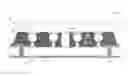
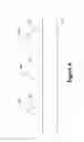
FIGS. 1A-1B depict an illustrative embodiment of a device 10 in accordance with one aspect of the present subject matter. The device 10 comprises a die 12 that is attached to an interposer or substrate 14, e.g., a printed circuit board. The terms “substrate” and “interposer” will be used interchangeably herein and they shall be understood to refer to any type of structure to which an integrated circuit die may be mounted. The die 12 comprises a plurality of schematically depicted solder balls 16 that are conductively coupled to conductive pads 17. The solder balls 16 have an illustrative oxide layer 20, e.g., tin oxide, formed on the outer surface thereof due to the manufacturing processes performed to form the solder balls 16. A plurality of piercing bond structures 22 are formed on the substrate 14. The piercing bond structures 22 are conductively coupled to illustrative wire traces or lines 24 that extend through vias 26 formed in the substrate 14. The wiring traces 24 are conductively coupled to illustrative contact pads 28 formed on the substrate 14. A layer of dielectric material 30 is also provided to electrically isolate various electrical components on the substrate 14. At least one anti-oxidation film 23 (see FIG. 1C) is provided on the piercing bond structures 22.
FIG. 1A depicts the situation wherein the die 12 is positioned proximate the substrate 14 prior to attachment. The die 12 may be coupled to the substrate 14 using a variety of known techniques, e.g., adhesives, epoxies, etc. In the depicted example, an amount of non-conductive paste 32 is positioned on the substrate 14. A non-conductive film may, in some applications, be applied in lieu of the non-conductive paste 32.
FIG. 1B depicts the device 10 at the point of fabrication wherein the die 12 has been conductively coupled to the substrate 14 by virtue of the conductive engagement between the piercing bond structures 22 and the solder balls 16. The piercing bond structures 22 pierce the oxide layer 20 and the solder ball 16 to thereby establish this conductive connection. Also note that FIG. 1B depicts an illustrative standoff structure 34 that may be employed if desired or needed to ensure that the die 12 is positioned a fixed distance from the substrate 14.
In attaching the die 12 to the substrate 14, the device 10 is heated and an illustrative downforce 40 is applied. The magnitude of the downforce 40 may vary depending upon the particular application. In one illustrative embodiment, the downforce 40 may range from approximately 2-12 kg. In some specific applications, a downforce 40 of approximately 8 kg may be employed. The device 10 is heated to a temperature above the melting point of the material of the solder ball 16, e.g., to a temperature ranging from approximately 190-210° C. The downforce 40 may be applied for a duration of 0.5-2 seconds, depending on the particular application. The article entitled “Instantaneous Fluxless Bonding of Au with Pb—Sn Solder in Ambient Atmosphere,” Journal of Applied Physics, Vol. 98, 034904 (2005) is hereby incorporated by reference in its entirety.
FIGS. 1C-1D are enlarged views of an illustrative solder ball 16 and piercing bond structure 22 prior to engagement (FIG. 1C) and after engagement (FIG. 1D). As mentioned previously, the piercing bond structure 22 has one or more anti-oxidation layers 23 formed on the structure 22 to prevent an oxide film from forming on the piercing bond structure 22. In the illustrative example depicted in FIGS. 1C-1D, the anti-oxidation layer 23 comprises a layer of gold 23A and a layer of nickel 23B. Of course, other materials may be employed. The layer of gold 23A may have a thickness of approximately 2.5 μm, while the layer of nickel 23B may have a thickness of approximately 0.3 μm.
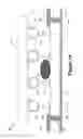
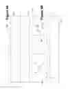
FIGS. 2A-2B schematically depict the reduced pitch between adjacent conductive structures that may result by use of the piercing bond structures 22 disclosed herein. FIG. 2A schematically depicts an illustrative conductive bond structures 90 that are commonly formed using known techniques. The conventional bond structures 90 have a substantially planar upper or contact surface 92. In FIG. 2A, the width of the contact surface 92 is designated “A,” the width of the sloped sidewalls 94, due to the isotropic nature of the etching process used to form the structures 90, is designated as “B” and the spacing between the structures 90 is designated as “C.” Thus, the pitch “P” for the conductive structure 90 would be A+2B+C. In contrast, the pitch (“P1”) between the piercing bond structures 22 shown in FIG. 2B would be equal to 2B+C. In short, using the techniques and piercing bond structures 22 disclosed herein, the pitch between conductive bonding structures (like the piercing bond structures 22 disclosed herein) may be substantially less as compared to prior art devices that employ bonding structures having a substantially planar or non-piercing upper surface 92, as shown in FIG. 2A. For example, using the piercing bond structures 22 described herein, the pitch “P1” may be approximately 60 μm minimum.
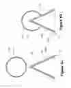
As shown in FIG. 3, the methodologies and piercing bond structures 22 disclosed herein may be employed with solder balls 16A, 16B, 16C of differing sizes. Thus, the piercing bond structures 22 described herein may be employed with a vast variety of different connection technologies and techniques.
The present subject matter may also be employed to control the offset between the die 12 and the printed circuit board 14. In general, all other things being equal, the greater the downforce 40, the less the distance between the die 12 and the printed circuit board 14. The temperature during the engagement process can also be employed to control the spacing between the die 12 and the printed circuit board 14. In general, the greater the temperature, the less the spacing between the die 12 and the printed circuit board 14.
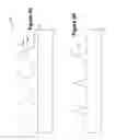
As shown in FIG. 4, the piercing bond structures 22 may have a variety of configurations for the piercing end 22A of the structure 22. For example, the piercing end 22A may be pointed, rounded or comprise multiple peaks as depicted on the piercing bond structures 22 in FIG. 4 (from left to right).
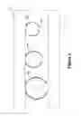
FIGS. 5A-5D depict one illustrative process flow for forming the piercing bond structures 22 described herein. Initially, as shown in FIG. 5A, a masking layer 80 is formed above a layer of conductive material 82. The masking layer 80 may be comprised of a variety of materials, e.g., a photoresist material, and it may be formed using traditional photolithography techniques. The layer of conductive material 82 may be comprised of a variety of different materials, e.g., gold, and it may be formed by a variety of known techniques, e.g., plating.
As shown in FIG. 5B, an anisotropic etching process 84 is performed to partially define conductive structures 86 having sloped sidewalls 87. The etching process 84 may be stopped at a point in time such that a portion 88 of the layer of conductive material 82 is not etched completely away. In some applications, stopping the etch process 84 so as to leave a remaining portion 88 of the layer of conductive material 82 may not be required. As shown in FIG. 5C, the masking layer 80 is removed, and an isotropic etching process 89 is performed until such time as the piercing bond structures 22 depicted in FIG. 5D are formed. Note that, in the illustrative embodiment depicted herein, the piercing bond structures 22 have a substantially triangular cross-sectional configuration and a substantially pointed end 22A. The end 22A of the piercing bond structure 22 is generally non-planar or non-flat, but it may take on other configurations. For example, FIG. 4 depicts various illustrative configurations for the end 22A of the piercing bond structures 22.
The particular embodiments disclosed above are illustrative only, as the invention may be modified and practiced in different but equivalent manners apparent to those skilled in the art having the benefit of the teachings herein. For example, the process steps set forth above may be performed in a different order. Furthermore, no limitations are intended to the details of construction or design herein shown, other than as described in the claims below. It is therefore evident that the particular embodiments disclosed above may be altered or modified and all such variations are considered within the scope and spirit of the invention. Accordingly, the protection sought herein is as set forth in the claims below.
Claims
1-20. (canceled)
21. A device comprising:
a substrate having a first side and a second side facing away from the first side;
a plurality of piercing bond structures at the first side of the substrate;
a plurality of contact pads at the second side of the substrate; and
a plurality of wiring traces electrically coupling the piercing bond structures with the contact pads.
22. The device of claim 21 wherein the piercing bond structures include an anti-oxidation material formed as an outer surface of the piercing bond structures.
23. The device of claim 22 wherein the anti-oxidation material is a first anti-oxidation material, the device further including a second anti-oxidation material over the first anti-oxidation material.
24. The device of claim 23 wherein the first anti-oxidation material is gold and the second anti-oxidation material is nickel.
25. The device of claim 21 wherein individual piercing bond structures have a first end facing the first side of the substrate and a second end facing away from the first end, and wherein the second ends are non-flat.
26. The device of claim 21 wherein the piercing bond structures have substantially triangular cross-sections.
27. The device of claim 21 wherein individual piercing bond structures have a first end facing the first side of the substrate and a second end facing away from the first end, and wherein the individual second ends have cross-sections selected from a group consisting of a pointed cross-section, a rounded cross-section, and a multiple-peak cross section.
28. The device of claim 21, further comprising a standoff structure at the first side of the substrate, wherein the standoff structure extends away from the first side of the substrate for a distance.
29. The device of claim 21, further comprising a non-conductive paste at the first side of the substrate.
30. The device of claim 21 wherein the substrate includes a via extending from the first side of the substrate to the second side of the substrate, wherein at least one wiring trace lines the via.
31. A device comprising:
a substrate having a first side and a second side facing away from the first side;
a piercing bond structure at the first side of the substrate, wherein the piercing bond structure has an outer surface that includes an anti-oxidation material;
a contact pad at the second side of the substrate;
a wiring trace electrically coupling the piercing bond structure with the contact pad;
a non-conductive paste at the first side of the substrate; and
a standoff structure at the first side of the substrate, wherein the standoff extends away from the first side of the substrate a predetermined distance.
32. The device of claim 31 wherein the anti-oxidation material is a first anti-oxidation material, the device further including a second anti-oxidation material over the first anti-oxidation material.
33. The device of claim 31 wherein the first anti-oxidation material is gold and the second anti-oxidation material is nickel.
34. The device of claim 31 wherein the piercing structure has a first end facing the first side of the substrate and a second end facing away from the first end, and wherein the second end has a pointed cross-section.
35. The device of claim 31 wherein the piercing structure has a first end facing the first side of the substrate and a second end facing away from the first end, and wherein the second end has a rounded cross-section.
36. The device of claim 31 wherein the piercing structure has a first end facing the first side of the substrate and a second end facing away from the first end, and wherein the second end has a cross-section with multiple peaks.
37. The device of claim 31 wherein the substrate includes a via extending from the first side of the substrate to the second side of the substrate, wherein the wiring trace and a dielectric material are inside the via.
38. The device of claim 31, further comprising a plurality of piercing bond structures at the first side of the substrate, the plurality of piercing bond structures having substantially triangular cross-sections.
39. The device of claim 31, further comprising a non-conductive paste at the first side of the substrate.
Images & Drawings included:


Sources:
- United States Patent and Trademark Office - verify current appl. status at the USPTO↗
Similar patent applications:
- » 20090152719
Methods of fluxless micro-piercing of solder balls, and resulting devices - » 20100264541
Methods of fluxless micro-piercing of solder balls, and resulting devices - » 20130234328
Methods of fluxless micro-piercing of solder balls, and resulting devices - » 20190019774
Methods of fluxless micro-piercing of solder balls, and resulting devices
Recent applications in this class:
- » 20250293190 2025-09-18
WAFER LEVEL CHIP SCALE PACKAGE HAVING VARYING THICKNESSES - » 20250259955 2025-08-14
METHOD FOR CHIP PACKAGING WITH HIGH-DENSITY CONNECTION LAYER, AND CHIP PACKAGING STRUCTURE - » 20250218998 2025-07-03
LOW TEMPERATURE SOLDER INTERCONNECT FOR PACKAGE PITCH SCALING - » 20250183211 2025-06-05
STRESS MITIGATING PILLAR BUMPS - » 20250167151 2025-05-22
SEMICONDUCTOR PACKAGE - » 20250157971 2025-05-15
THREE-DIMENSIONAL CHIP STACK PREPARING METHOD AND THREE-DIMENSIONAL CHIP STACKING STRUCTURE - » 20250157970 2025-05-15
FLIP CHIP STRUCTURE AND CIRCUIT BOARD THEREOF - » 20250149489 2025-05-08
Multi-Die Fine Grain Integrated Voltage Regulation - » 20250140726 2025-05-01
SEMICONDUCTOR PACKAGE - » 20250140725 2025-05-01
BUMP ARRANGEMENT OF INTEGRATED CIRCUITS FOR FLIP CHIP BONDING
Recent applications for this Assignee:
- » 20250294729 2025-09-18
Memory Circuitry And Methods Used In Forming Memory Circuitry - » 20250293722 2025-09-18
HIGH SPEED RECEIVER FOR MULTI-GIGA HERTZ OPERATIONS - » 20250292844 2025-09-18
Validating Uninitialized Usage-Based-Disturbance Data - » 20250292836 2025-09-18
Memory Arrays Comprising Strings Of Memory Cells And Methods Used In Forming A Memory Array Comprising Strings Of Memory Cells - » 20250292835 2025-09-18
Memory Arrays Comprising Strings Of Memory Cells And Methods Used In Forming A Memory Array Comprising Strings Of Memory Cells - » 20250292821 2025-09-18
Multiple-Row Refresh for Usage-Based Disturbance Mitigation - » 20250291671 2025-09-18
APPARATUSES AND METHODS FOR ADJUSTING REFRESH RATES ON MEMORY DEVICES OF A MODULE - » 20250284540 2025-09-11
Broadcasting a Host-Controlled Parameter to Circuitry Distributed at a Local-Bank Level for Usage-Based-Disturbance Mitigation - » 20250280546 2025-09-04
Integrated Circuitry, Array of Cross-Point Memory Cells, Method Used in Forming Integrated Circuitry - » 20250280539 2025-09-04
Integrated Circuitry Comprising a Memory Array Comprising Strings of Memory Cells and Methods Used in Forming a Memory Array Comprising Strings of Memory Cells