Semiconductor package
US20060237840A1
2006-10-26
11/405,825
2006-04-18
✅ Patent granted
US 7,230,333 B2
2007-06-12
-
-
Nitin Parekh
2026-04-18
Abstract:
A semiconductor package that includes a conductive can, a power semiconductor device electrically and mechanically attached to the inside surface of the can, and an IC semiconductor device copackaged with the power semiconductor device inside the can.
Assignee:
- INTERNATIONAL RECTIFIER CORPORATION 879 🇺🇸 EL SEGUNDO, CA, United States
Interested in similar patents?
Get notified when new applications in this technology area are published.
Classification:
H01L23/12 IPC
Details of semiconductor or other solid state devices Mountings, e.g. non-detachable insulating substrates
H01L23/043 IPC
Details of semiconductor or other solid state devices; Containers; Seals characterised by the shape of the container or parts, e.g. caps, walls the container being a hollow construction and having a conductive base as a mounting as well as a lead for the semiconductor body
H01L23/10 IPC
Details of semiconductor or other solid state devices; Containers; Seals characterised by the material or arrangement of seals between parts, e.g. between cap and base of the container or between leads and walls of the container
H01L29/00 IPC
Semiconductor devices adapted for rectifying, amplifying, oscillating or switching, or capacitors or resistors with at least one potential-jump barrier or surface barrier, e.g. PN junction depletion layer or carrier concentration layer; Details of semiconductor bodies or of electrodes thereof; Multistep manufacturing processes therefor
H01L2924/1305 » CPC further
Indexing scheme for arrangements or methods for connecting or disconnecting semiconductor or solid-state bodies as covered by; Details of semiconductor or other solid state devices to be connected; Device type; Discrete devices, e.g. 3 terminal devices; Transistor Bipolar Junction Transistor [BJT]
H01L2924/00 » CPC further
Indexing scheme for arrangements or methods for connecting or disconnecting semiconductor or solid-state bodies as covered by
H01L2224/8485 » CPC further
Indexing scheme for arrangements for connecting or disconnecting semiconductor or solid-state bodies and methods related thereto as covered by; Methods for connecting semiconductor or other solid state bodies using means for bonding being attached to, or being formed on, the surface to be connected using a strap connector; Bonding techniques using a polymer adhesive, e.g. an adhesive based on silicone, epoxy, polyimide, polyester
H01L2224/8385 » CPC further
Indexing scheme for arrangements for connecting or disconnecting semiconductor or solid-state bodies and methods related thereto as covered by; Methods for connecting semiconductor or other solid state bodies using means for bonding being attached to, or being formed on, the surface to be connected using a layer connector; Bonding techniques using a polymer adhesive, e.g. an adhesive based on silicone, epoxy, polyimide, polyester
H01L2924/00014 » CPC further
Indexing scheme for arrangements or methods for connecting or disconnecting semiconductor or solid-state bodies as covered by; Technical content checked by a classifier the subject-matter covered by the group, the symbol of which is combined with the symbol of this group, being disclosed without further technical details
H01L23/34 IPC
Details of semiconductor or other solid state devices Arrangements for cooling, heating, ventilating or temperature compensation ; Temperature sensing arrangements
H01L24/40 » CPC main
Arrangements for connecting or disconnecting semiconductor or solid-state bodies; Methods or apparatus related thereto; Means for bonding being attached to, or being formed on, the surface to be connected, e.g. chip-to-package, die-attach, "first-level" interconnects; Manufacturing methods related thereto; Strap connectors, e.g. copper straps for grounding power devices; Manufacturing methods related thereto; Structure, shape, material or disposition of the strap connectors after the connecting process of an individual strap connector
H01L23/04 » CPC further
Details of semiconductor or other solid state devices; Containers; Seals characterised by the shape of the container or parts, e.g. caps, walls
H01L23/06 » CPC further
Details of semiconductor or other solid state devices; Containers; Seals characterised by the material of the container or its electrical properties
H01L23/13 » CPC further
Details of semiconductor or other solid state devices; Mountings, e.g. non-detachable insulating substrates characterised by the shape
H01L23/14 » CPC further
Details of semiconductor or other solid state devices; Mountings, e.g. non-detachable insulating substrates characterised by the material or its electrical properties
H01L23/492 » CPC further
Details of semiconductor or other solid state devices; Arrangements for conducting electric current to or from the solid state body in operation, e.g. leads, terminal arrangements ; Selection of materials therefor consisting of soldered constructions Bases or plates or solder therefor
H01L23/4924 » CPC further
Details of semiconductor or other solid state devices; Arrangements for conducting electric current to or from the solid state body in operation, e.g. leads, terminal arrangements ; Selection of materials therefor consisting of soldered constructions; Bases or plates or solder therefor characterised by the materials
H01L23/49548 » CPC further
Details of semiconductor or other solid state devices; Arrangements for conducting electric current to or from the solid state body in operation, e.g. leads, terminal arrangements ; Selection of materials therefor consisting of soldered constructions; Lead-frames or other flat leads; Geometry of the lead-frame Cross section geometry
H01L23/49558 » CPC further
Details of semiconductor or other solid state devices; Arrangements for conducting electric current to or from the solid state body in operation, e.g. leads, terminal arrangements ; Selection of materials therefor consisting of soldered constructions; Lead-frames or other flat leads; Geometry of the lead-frame Insulating layers on lead frames, e.g. bridging members
H01L23/49582 » CPC further
Details of semiconductor or other solid state devices; Arrangements for conducting electric current to or from the solid state body in operation, e.g. leads, terminal arrangements ; Selection of materials therefor consisting of soldered constructions; Lead-frames or other flat leads characterised by the materials of the lead frames or layers thereon Metallic layers on lead frames
H01L23/4985 » CPC further
Details of semiconductor or other solid state devices; Arrangements for conducting electric current to or from the solid state body in operation, e.g. leads, terminal arrangements ; Selection of materials therefor consisting of soldered constructions; Leads, on insulating substrates, Flexible insulating substrates
H01L24/24 » CPC further
Arrangements for connecting or disconnecting semiconductor or solid-state bodies; Methods or apparatus related thereto; Means for bonding being attached to, or being formed on, the surface to be connected, e.g. chip-to-package, die-attach, "first-level" interconnects; Manufacturing methods related thereto; High density interconnect [HDI] connectors; Manufacturing methods related thereto; Structure, shape, material or disposition of the high density interconnect connectors after the connecting process of an individual high density interconnect connector
H01L24/34 » CPC further
Arrangements for connecting or disconnecting semiconductor or solid-state bodies; Methods or apparatus related thereto; Means for bonding being attached to, or being formed on, the surface to be connected, e.g. chip-to-package, die-attach, "first-level" interconnects; Manufacturing methods related thereto Strap connectors, e.g. copper straps for grounding power devices; Manufacturing methods related thereto
H01L24/36 » CPC further
Arrangements for connecting or disconnecting semiconductor or solid-state bodies; Methods or apparatus related thereto; Means for bonding being attached to, or being formed on, the surface to be connected, e.g. chip-to-package, die-attach, "first-level" interconnects; Manufacturing methods related thereto; Strap connectors, e.g. copper straps for grounding power devices; Manufacturing methods related thereto Structure, shape, material or disposition of the strap connectors prior to the connecting process
H01L24/37 » CPC further
Arrangements for connecting or disconnecting semiconductor or solid-state bodies; Methods or apparatus related thereto; Means for bonding being attached to, or being formed on, the surface to be connected, e.g. chip-to-package, die-attach, "first-level" interconnects; Manufacturing methods related thereto; Strap connectors, e.g. copper straps for grounding power devices; Manufacturing methods related thereto; Structure, shape, material or disposition of the strap connectors prior to the connecting process of an individual strap connector
H01L24/82 » CPC further
Arrangements for connecting or disconnecting semiconductor or solid-state bodies; Methods or apparatus related thereto; Methods for connecting semiconductor or other solid state bodies using means for bonding being attached to, or being formed on, the surface to be connected by forming build-up interconnects at chip-level, e.g. for high density interconnects [HDI]
H01L24/83 » CPC further
Arrangements for connecting or disconnecting semiconductor or solid-state bodies; Methods or apparatus related thereto; Methods for connecting semiconductor or other solid state bodies using means for bonding being attached to, or being formed on, the surface to be connected using a layer connector
H01L24/84 » CPC further
Arrangements for connecting or disconnecting semiconductor or solid-state bodies; Methods or apparatus related thereto; Methods for connecting semiconductor or other solid state bodies using means for bonding being attached to, or being formed on, the surface to be connected using a strap connector
H01L25/165 » CPC further
Assemblies consisting of a plurality of individual semiconductor or other solid state devices ; Multistep manufacturing processes thereof the devices being of types provided for in two or more different main groups of - , e.g. forming hybrid circuits Containers
H01L2224/0603 » CPC further
Indexing scheme for arrangements for connecting or disconnecting semiconductor or solid-state bodies and methods related thereto as covered by; Means for bonding being attached to, or being formed on, the surface to be connected, e.g. chip-to-package, die-attach, "first-level" interconnects; Manufacturing methods related thereto; Bonding areas; Manufacturing methods related thereto; Structure, shape, material or disposition of the bonding areas prior to the connecting process of a plurality of bonding areas; Structure Bonding areas having different sizes, e.g. different heights or widths
H01L2224/73153 » CPC further
Indexing scheme for arrangements for connecting or disconnecting semiconductor or solid-state bodies and methods related thereto as covered by; Means for bonding being of different types provided for in two or more of groups; Location prior to the connecting process on different surfaces Bump and layer connectors
H01L2224/73253 » CPC further
Indexing scheme for arrangements for connecting or disconnecting semiconductor or solid-state bodies and methods related thereto as covered by; Means for bonding being of different types provided for in two or more of groups; Location after the connecting process on different surfaces Bump and layer connectors
H01L2224/76155 » CPC further
Indexing scheme for arrangements for connecting or disconnecting semiconductor or solid-state bodies and methods related thereto as covered by; Apparatus for manufacturing arrangements for connecting or disconnecting semiconductor or solid-state bodies and for methods related thereto; Apparatus for connecting with build-up interconnects; Means for depositing; Means for direct writing Jetting means, e.g. ink jet
H01L2224/82102 » CPC further
Indexing scheme for arrangements for connecting or disconnecting semiconductor or solid-state bodies and methods related thereto as covered by; Methods for connecting semiconductor or other solid state bodies using means for bonding being attached to, or being formed on, the surface to be connected by forming build-up interconnects at chip-level, e.g. for high density interconnects [HDI]; Forming a build-up interconnect by additive methods, e.g. direct writing using jetting, e.g. ink jet
H01L2224/84801 » CPC further
Indexing scheme for arrangements for connecting or disconnecting semiconductor or solid-state bodies and methods related thereto as covered by; Methods for connecting semiconductor or other solid state bodies using means for bonding being attached to, or being formed on, the surface to be connected using a strap connector; Bonding techniques Soldering or alloying
H01L2924/01004 » CPC further
Indexing scheme for arrangements or methods for connecting or disconnecting semiconductor or solid-state bodies as covered by; Chemical elements Beryllium [Be]
H01L2924/01005 » CPC further
Indexing scheme for arrangements or methods for connecting or disconnecting semiconductor or solid-state bodies as covered by; Chemical elements Boron [B]
H01L2924/01013 » CPC further
Indexing scheme for arrangements or methods for connecting or disconnecting semiconductor or solid-state bodies as covered by; Chemical elements Aluminum [Al]
H01L2924/01027 » CPC further
Indexing scheme for arrangements or methods for connecting or disconnecting semiconductor or solid-state bodies as covered by; Chemical elements Cobalt [Co]
H01L2924/01029 » CPC further
Indexing scheme for arrangements or methods for connecting or disconnecting semiconductor or solid-state bodies as covered by; Chemical elements Copper [Cu]
H01L2924/01033 » CPC further
Indexing scheme for arrangements or methods for connecting or disconnecting semiconductor or solid-state bodies as covered by; Chemical elements Arsenic [As]
H01L2924/01045 » CPC further
Indexing scheme for arrangements or methods for connecting or disconnecting semiconductor or solid-state bodies as covered by; Chemical elements Rhodium [Rh]
H01L2924/01047 » CPC further
Indexing scheme for arrangements or methods for connecting or disconnecting semiconductor or solid-state bodies as covered by; Chemical elements Silver [Ag]
H01L2924/01078 » CPC further
Indexing scheme for arrangements or methods for connecting or disconnecting semiconductor or solid-state bodies as covered by; Chemical elements Platinum [Pt]
H01L2924/01079 » CPC further
Indexing scheme for arrangements or methods for connecting or disconnecting semiconductor or solid-state bodies as covered by; Chemical elements Gold [Au]
H01L2924/01082 » CPC further
Indexing scheme for arrangements or methods for connecting or disconnecting semiconductor or solid-state bodies as covered by; Chemical elements Lead [Pb]
H01L2924/01084 » CPC further
Indexing scheme for arrangements or methods for connecting or disconnecting semiconductor or solid-state bodies as covered by; Chemical elements Polonium [Po]
H01L2924/014 » CPC further
Indexing scheme for arrangements or methods for connecting or disconnecting semiconductor or solid-state bodies as covered by; Alloys Solder alloys
H01L2924/05432 » CPC further
Indexing scheme for arrangements or methods for connecting or disconnecting semiconductor or solid-state bodies as covered by; Oxides composed of metals from groups of the periodic table 13th Group AlO
H01L2924/0635 » CPC further
Indexing scheme for arrangements or methods for connecting or disconnecting semiconductor or solid-state bodies as covered by; Polymers Acrylic polymer
H01L2924/0665 » CPC further
Indexing scheme for arrangements or methods for connecting or disconnecting semiconductor or solid-state bodies as covered by; Polymers Epoxy resin
H01L2924/07025 » CPC further
Indexing scheme for arrangements or methods for connecting or disconnecting semiconductor or solid-state bodies as covered by; Polymers; Polyamine or polyimide Polyimide
H01L2924/0715 » CPC further
Indexing scheme for arrangements or methods for connecting or disconnecting semiconductor or solid-state bodies as covered by; Polymers Polysiloxane
H01L2924/13055 » CPC further
Indexing scheme for arrangements or methods for connecting or disconnecting semiconductor or solid-state bodies as covered by; Details of semiconductor or other solid state devices to be connected; Device type; Discrete devices, e.g. 3 terminal devices; Transistor; Bipolar Junction Transistor [BJT] Insulated gate bipolar transistor [IGBT]
H01L2924/13091 » CPC further
Indexing scheme for arrangements or methods for connecting or disconnecting semiconductor or solid-state bodies as covered by; Details of semiconductor or other solid state devices to be connected; Device type; Discrete devices, e.g. 3 terminal devices; Transistor; Field-effect transistor [FET] Metal-Oxide-Semiconductor Field-Effect Transistor [MOSFET]
H01L2924/14 » CPC further
Indexing scheme for arrangements or methods for connecting or disconnecting semiconductor or solid-state bodies as covered by; Details of semiconductor or other solid state devices to be connected; Device type Integrated circuits
Y10T29/49117 » CPC further
Metal working; Method of mechanical manufacture; Electrical device making Conductor or circuit manufacturing
Y10T29/49126 » CPC further
Metal working; Method of mechanical manufacture; Electrical device making; Conductor or circuit manufacturing; On flat or curved insulated base, e.g., printed circuit, etc. Assembling bases
Y10T29/49128 » CPC further
Metal working; Method of mechanical manufacture; Electrical device making; Conductor or circuit manufacturing; On flat or curved insulated base, e.g., printed circuit, etc. Assembling formed circuit to base
Y10T29/4913 » CPC further
Metal working; Method of mechanical manufacture; Electrical device making; Conductor or circuit manufacturing; On flat or curved insulated base, e.g., printed circuit, etc. Assembling to base an electrical component, e.g., capacitor, etc.
Y10T29/49147 » CPC further
Metal working; Method of mechanical manufacture; Electrical device making; Conductor or circuit manufacturing; On flat or curved insulated base, e.g., printed circuit, etc. Assembling terminal to base
Y10T29/49155 » CPC further
Metal working; Method of mechanical manufacture; Electrical device making; Conductor or circuit manufacturing; On flat or curved insulated base, e.g., printed circuit, etc. Manufacturing circuit on or in base
Y10T29/49174 » CPC further
Metal working; Method of mechanical manufacture; Electrical device making; Conductor or circuit manufacturing Assembling terminal to elongated conductor
Description
RELATED APPLICATIONThis application is based on and claims benefit of United States Provisional Application No. 60/674,162, filed on Apr. 21, 2005, entitled Semiconductor Package, to which a claim of priority is hereby made and the disclosure of which is incorporated by reference.
BACKGROUND OF THE INVENTIONThe present invention relates to semiconductor packages.
In the recent years, chip-scale packages have become very important. The present invention relates to power semiconductor packages and methods of manufacturing power semiconductor packages.
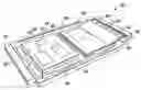
Referring to FIGS. 1-4, a package 10 according to the prior art includes a conductive can 12, and a power semiconductor die 14. Can 12 is typically formed with an electrically conductive material such as copper or a copper-based alloy, and may be coated with silver, gold or the like. Die 14 may be a vertical conduction type power semiconductor MOSFET having its drain electrode 16 electrically and mechanically attached to an interior surface of can 12 by a conductive adhesive 18 such as solder or a conductive epoxy (e.g. silver epoxy). Source electrode 20, and gate electrode 22 of die 14 (which are disposed on a surface opposite to the drain electrode) each includes a solderable body which facilitates its direct connection to a respective conductive pad 24, 26 of a circuit board 28 by a conductive adhesive (e.g. solder or conductive epoxy) as illustrated by FIG. 4. Note that die 14 further includes passivation body 30 which partially covers source electrode 20 and gate electrode 22, but includes openings to allow access at least to the solderable portions thereof for electrical connection. Further note that in package 10 conductive can 12 includes web portion 13 (to which die 14 is electrically and mechanically connected), wall 15 surrounding web portion 13, and two oppositely disposed rails 32 extending from wall 15 each configured for. connection to a respective conductive pad 34 on circuit board 28. Also, note that die 14 is spaced from wall 13 of can 12; i.e. wall 13 surrounds die 14. Thus, a moat 36 is present between die 14 and wall 13.
In a package according to the prior art, source electrode 20, and gate electrode 22 are soldered down by the user. Specifically, the user applies solder to, for example, the pads of a circuit board, and the electrodes of the die are attached to the pads by the solder so placed.
A package as described above is disclosed in U.S. Pat. No. 6,624,522.
DESCRIPTION OF PROCESS FOR FABRICATING DEVICEIn some applications it is desirable to co-package two or more die in the same package. For example, it is desirable to co-package a power semiconductor die such as a power MOSFET with an IC die or the like for driving the die.
A semiconductor package according to the present invention includes a can-shaped conductive clip having an interior surface, a dielectric body disposed over at least a portion of the interior surface of the conductive clip, at least one I/O terminal, a conductive pad, a track connecting the pad to the I/O terminal, an IC having at least one pad electrically connected to the die pad, and a power semiconductor device having at least one power electrode electrically and mechanically connected to another portion of the interior surface of the conductive clip.
In a package according to the preferred embodiment of the present invention the clip is configured to receive a power MOSFET with an IC die for driving the power die.
Other features and advantages of the present invention will become apparent from the following description of the invention which refers to the accompanying drawings.
BRIEF DESCRIPTION OF THE FIGURESFIG. 1 is a perspective view of a package according to prior art.
FIG. 2 is another perspective view of the package of FIG. 1.
FIG. 3 is a cross-sectional view of the package of FIG. 1 along line 3-3 in FIG. 2.
FIG. 4 shows the package of FIG. 1 as assembled on a circuit board.
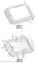
FIG. 5 shows a perspective bottom view of a package according to the present invention.
FIGS. 6-8 illustrate selected steps in the fabrication of a package according to the present invention.
DETAILED DESCRIPTION OF EMBODIMENTReferring next to FIG. 5, a package 38 according to the preferred embodiment of the present invention includes conductive can 40, which includes a web portion 42, a wall 44 surrounding web portion 42, a first rail 46 disposed at one side of wall 44, and second rail 48 disposed at a second side of wall 44 opposite the first side. Note that according to one aspect of the present invention second rail 48 is spaced laterally further away than first wall 46 by a lateral lip portion 50. Conductive can 48 is preferably made from copper or a copper alloy, and may be coated with silver, gold or the like. Package 38 further includes a power semiconductor device 52. Power semiconductor device is preferably a power MOSFET that includes identical or similar features as die 14 in a semiconductor package; however, device 52 may also be an IGBT or the like. Specifically, device 52 includes source electrode 20, a gate electrode 22 on one surface thereof, and drain electrode (not shown) on an opposite surface thereof electrically and mechanically connected to web portion 42 by a conductive adhesive 54. Note that similar to die 14, a passivation body 56 is disposed on a surface of device 52 and surrounds source electrode 20, and gate electrode 22 in the same manner as described above with reference to the prior art. Note that source electrode 20, and gate electrode 22 may be rendered solderable for direct connection with a conductive adhesive or the like to a conductive pad of, for example, a circuit board.
Package 38 further includes an integrated circuit semiconductor device (IC) 58. In the preferred embodiment, IC 58 includes a driver circuit that is capable of driving power MOSFET 52. IC 58 is electrically connected to a plurality of input/output terminals (I/O) terminals 60. I/O terminals 60 reside over an insulation body disposed on lip portion 50. The purpose of I/O terminals 60 is to transmit input signals to IC 58, and receive output signals from IC 58. Note that preferably I/O terminals 60 are coplanar with first and second tracks 46, 48. As a result, when assembled, I/O terminals 60 may be electrically and mechanically connected to corresponding pads on a circuit board (e.g. by a conductive adhesive such as solder or conductive epoxy) that are coplanar with and adjacent to a pad designated for receiving second rail 48.
Referring next to FIGS. 6-8, to fabricate package 38 first a dielectric body 62 is deposited on a portion of web portion 42 extending along a portion of wall 44 and lip 50. Dielectric body 62 is preferably made from a polymer-based material, and can be deposited through stenciling, drop-on-demand deposition, or any other suitable method. Drop-on-demand deposition is disclosed in U.S. patent application Ser. No. 11/367,725, assigned to the assignee of the present invention, and incorporated herein by this reference. Drop-on-demand deposition is a preferred method for the advantages set forth in U.S. patent application Ser. No. 11/367,725.
Dielectrics capable of the isolation desired for a package according to the present invention have been used in the production of plasma panel displays. Such dielectric materials include dielectric particles loaded in an organic base, which may be any of the following depending upon the application requirements: epoxy, acrylic based (acrylate), polyimide or organopolysiloxane. UV curing materials are preferred to reduce the process time, although other materials such as thermally curable materials may be used without deviating from the present invention. The dielectric material would be typically a metal oxide such as alumina or aluminum nitride. Preferably, the dielectric material has a low and very controlled particle size to allow for drop-on-demand deposition.
Referring next to FIG. 7, a plurality of conductive input/output leads (I/O leads) are formed on dielectric body 62. Each I/O lead includes a conductive pad 64 which is electrically connected to a respective I/O terminal 60 via a respective conductive track 66. I/O leads can also be formed through any printing method such as stenciling, or deposition method such as drop-on-demand deposition. In one alternative embodiment, an organic based trace layer can be first deposited and cured. The cured trace will then form a seed layer for the construction of I/O pads 64, tracks, and I/O terminals 60.
The material used for forming I/O leads and I/O terminals 60 may be a polymer that is impregnated with micronized, highly conductive particles. The dispersion of micronized, highly conductive particles within a polymer matrix can allow for relatively low resistance I/O leads and I/O terminals suitable for carrying signals to and from IC 58.
The conductive materials suitable for a package according to the present invention should be very similar in formulation to the dielectrics regarding the base materials. The conductive micronized fillers tend to be materials that are both highly conductive and have low tendencies to oxidize. Typical materials deemed suitable include gold, silver, platinum, rhodium etc, or combinations thereof.
Alternatively, the conductive material may be a mixture of reflowing (solders) and non-reflowing (metal particles) mixed in with a fluid to form a slurry, which is then printed to form a reflowable, fusible material, similar to the solder paste referred to above and disclosed in U.S. patent application Ser. No. 11/367,725. The alternative conductive material may increase the choices of metals, as the fluid used for the slurry could be used to reduce or protect the metals from oxidation.
Referring next to FIG. 8, a protective body 68 is deposited over at least conductive tracks 66. Note that pads 64, and terminals 60 remain exposed. Protective body 68 may be a solder resist material; i.e. a material that is unwettable by liquid solder, and may serve as a passivation. Preferably, protective body 68 is polymer-based. Protective body 68 may be printed using any known method such a stenciling, or deposited using drop-on-demand deposition.
Thereafter, a thick layer of conductive adhesive material is printed onto I/O pads 64 to be used as a die-bonding medium for IC 58. At the same time a highly solvent thinned, low resin loaded slurry material is printed onto the I/O terminals 60. The slurry material acts as a base layer for tinning or possible plating.
Next, device 52 and IC 58 are installed. Specifically, with a conductive adhesive the drain electrode of device 52 is electrically and mechanically connected to web portion 42 of can 40, and the electrodes (not shown) of IC 58 are electrically and mechanically connected to pads 64 using a conductive adhesive such as solder or a conductive epoxy, thereby realizing package 38 as illustrated in FIG. 5.
In one preferred embodiment, conductive epoxy is used for the connection of IC 58 and device 52. Specifically, conductive epoxy is deposited on web 42, and on I/O pads, device 52 and IC 58 are placed on the conductive epoxy deposits, and the arrangement is subject to a curing step. Optionally, a solder paste, such as the solder paste disclosed in U.S. patent application Ser. No. 10/970,165, is then deposited onto source electrode 20 and gate electrode 22 of device 52, and also I/O terminals 60. The arrangement is then subjected to a reflow heating step followed by a cleaning step. With or without the solder paste, optionally, IC 58 may be then underfilled using a volatile free organopolysiloxane, and the whole assembly (except for rails 46,48, I/O terminals 60, source electrode 20, and gate electrode 22) is covered with an organopolysiloxane. The assembly is then subjected to an appropriate curing step. As a result, IC 58 can be electrically connected to device 52 through conductive tracks on a circuit board, once package 38 is assembled in place.
Although the present invention has been described in relation to particular embodiments thereof, many other variations and modifications and other uses will become apparent to those skilled in the art.
Claims
What is claimed is:1. A semiconductor package comprising:
a conductive clip having an interior surface;
a dielectric body disposed over at least a portion of said interior surface of said conductive clip;
at least one I/O terminal;
a conductive pad;
a track connecting said pad to said I/O terminal;
an IC having at least one pad electrically connected to said die pad; and
a power semiconductor device having at least one power electrode electrically and mechanically connected to another portion of said interior surface of said conductive clip.
2. The package of claim 1, wherein said power semiconductor device is a power MOSFET.
3. The package of claim 1, wherein said power semiconductor device is an IGBT.
4. The package of claim 1, wherein said IC includes a driver circuit for driving said power semiconductor device.
5. The package of claim 1, wherein said conductive clip is can-shaped.
6. The package of claim 1, wherein said conductive clip is comprised of copper.
7. The package of claim 1, wherein said conductive clip is plated with either gold or silver.
8. The package of claim 1, further comprising a solder resist body covering at least said track.
9. The package of claim 1, wherein said dielectric body is comprised of a polymer.
10. A process for fabricating a semiconductor package comprising:
depositing a dielectric body over a portion of an interior surface of a conductive clip;
forming at least one I/O lead over said dielectric body, said I/O lead including a conductive pad portion, an I/O terminal, and a track connecting said conductive pad to said I/O terminal;
connecting an electrode of an IC to said conductive pad portion;
electrically and mechanically connecting a power electrode of a power semiconductor device to said interior surface of said conductive clip.
11. The process of claim 10, wherein said dielectric body is drop-on-demand deposited.
12. The process of claim 10, wherein said I/O lead is drop-on-demand deposited.
13. The process of claim 10, further comprising depositing a solder resist over at least a portion of said terminal.
14. The process of claim 13, wherein said solder resist is drop-on-demand deposited.
15. The process of claim 10, wherein said power semiconductor device is a power MOSFET.
16. The process of claim 10, wherein said power semiconductor device is an IGBT.
17. The process of claim 10, wherein said IC includes a driver circuit for driving said power semiconductor device.
18. The process of claim 10, wherein said conductive clip is can-shaped.
19. The process of claim 10, wherein said conductive clip is comprised of copper.
20. The process of claim 10, wherein said conductive clip is plated with either gold or silver.
21. The process of claim 10, wherein said dielectric body is comprised of a polymer.
Images & Drawings included:


Sources:
- United States Patent and Trademark Office - verify current appl. status at the USPTO↗
Similar patent applications:
- » 20210343617
Semiconductor devices including a lower semiconductor package, an upper semiconductor package on the lower semiconductor package, and a connection pattern between the lower semiconductor package and the upper semiconductor package - » 20230207416
Semiconductor devices including a lower semiconductor package, an upper semiconductor package on the lower semiconductor package, and a connection pattern between the lower semiconductor package and the upper semiconductor package - » 20110079890
Semiconductor package, semiconductor package structure including the semiconductor package, and mobile phone including the semiconductor package structure - » 20250149527
SEMICONDUCTOR PACKAGE, SEMICONDUCTOR PACKAGE INTERMEDIATE, REDISTRIBUTION LAYER CHIP, REDISTRIBUTION LAYER CHIP INTERMEDIATE, METHOD OF MANUFACTURING SEMICONDUCTOR PACKAGE, AND METHOD OF MANUFACTURING SEMICONDUCTOR PACKAGE INTERMEDIATE - » 20100213620
Manufacturing method of substrate for a semiconductor package, manufacturing method of semiconductor package, substrate for a semiconductor package and semiconductor package - » 20130309818
Manufacturing method of substrate for a semiconductor package, manufacturing method of semiconductor package, substrate for a semiconductor package and semiconductor package - » 20120064666
MANUFACTURING METHOD OF SUBSTRATE FOR A SEMICONDUCTOR PACKAGE, MANUFACTURING METHOD OF SEMICONDUCTOR PACKAGE, SUBSTRATE FOR A SEMICONDUCTOR PACKAGE AND SEMICONDUCTOR PACKAGE - » 20190267315
Method of manufacturing semiconductor package substrate and semiconductor package substrate manufactured using the method, and method of manufacturing semiconductor package and semiconductor package manufactured using the method - » 20110014748
Semiconductor packages, stacked semiconductor packages, and methods of manufacturing the semiconductor packages and the stacked semiconductor packages - » 20080157394
Semiconductor packages, stacked semiconductor packages, and methods of manufacturing the semiconductor packages and the stacked semiconductor packages
Recent applications in this class:
- » 20250286011 2025-09-11
SEMICONDUCTOR PACKAGE WITH HYBRID INTERCONNECT CLIP - » 20250279388 2025-09-04
SEMICONDUCTOR DEVICE - » 20250253284 2025-08-07
Multi-Die Integrated Circuit Device with a Spark Gap - » 20250246572 2025-07-31
CLIP DESIGN AND METHOD OF CONTROLLING CLIP POSITION - » 20250233099 2025-07-17
SEMICONDUCTOR DEVICE AND METHOD FOR MANUFACTURING SEMICONDUCTOR DEVICE - » 20250210579 2025-06-26
POWER STAGE DEVICE CLIP - » 20250192093 2025-06-12
SEMICONDUCTOR DEVICE AND METHODS OF MANUFACTURING SEMICONDUCTOR DEVICEs - » 20250183219 2025-06-05
SEMICONDUCTOR PACKAGES WITH CHIP STACK - » 20250132282 2025-04-24
CONTACT DEVICE AND POWER MODULE ARRANGEMENT - » 20250118699 2025-04-10
SEMICONDUCTOR DEVICE
Recent applications for this Assignee:
- » 20150130036 2015-05-14
Semiconductor package with low profile switch node integrated heat spreader - » 20150037965 2015-02-05
Fabrication of III-nitride semiconductor device and related structures - » 20150008572 2015-01-08
Power semiconductor package with multiple dies - » 20150001599 2015-01-01
Power semiconductor package with non-contiguous, multi-section conductive carrier - » 20140353680 2014-12-04
Gallium nitride semiconductor structures with compositionally-graded transition layer - » 20140339686 2014-11-20
Group III-V device with a selectively modified impurity concentration - » 20140339651 2014-11-20
Semiconductor device with a field plate double trench having a thick bottom dielectric - » 20140332879 2014-11-13
Power semiconductor device with reduced on-resistance and increased breakdown voltage - » 20140327014 2014-11-06
III-nitride rectifier package - » 20140319665 2014-10-30
Power semiconductor package