SPANSION LLC
Sunnyvale, California
United States
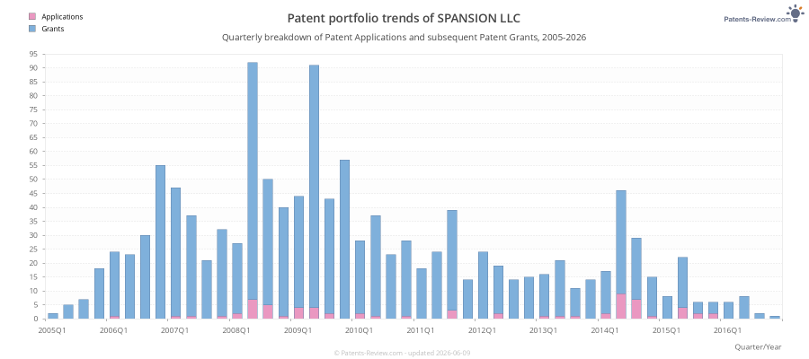
1,241
2016-09-22
1,173
2017-11-07
Top Inventors for applications by SPANSION LLC
These are the the leading inventors for applications assigned to SPANSION LLC:
- Kuo-Tung CHANG 77 Saratoga, CA United States
- Shenqing FANG 69 Fremont, CA United States
- Angela T. Hui 37 Fremont, CA United States
- Minh VAN NGO 35 Fremont, CA United States
- Hiroyuki KINOSHITA 35 San Jose, CA United States
- Hidehiko Shiraiwa 35 San Jose, CA United States
- Wei Zheng 34 Santa Clara, CA United States
- Mark Randolph 31 San Jose, CA United States
- Ning Cheng 30 San Jose, CA United States
- Zhizheng LIU 29 San Jose, CA United States
- YouSeok SUH 28 Cupertino, CA United States
- Ashot Melik-Martirosian 27 Sunnyvale, CA United States
- Yi HE 27 Fremont, CA United States
- Sameer HADDAD 26 San Jose, CA United States
- Nian Yang 26 Mountain View, CA United States
- Chun CHEN 25 San Jose, CA United States
- Angela HUI 24 Fremont, CA United States
- Kouichi MEGURO 24 Tokyo, Japan
- Masanori ONODERA 24 Tokyo, Japan
- Masaru YANO 22 Tokyo, Japan
- Richard Fastow 21 Cupertino, CA United States
- Timothy Thurgate 21 Sunnyvale, CA United States
- Unsoon Kim 20 San Jose, CA United States
- Rinji Sugino 20 San Jose, CA United States
- Chungho Lee 20 Sunnyvale, CA United States
- Meng Ding 20 Sunnyvale, CA United States
- Steven AVANZINO 19 Cupertino, CA United States
- Suzette K. Pangrle 18 Cupertino, CA United States
- Hagop Nazarian 18 San Jose, CA United States
- Kazuhiro Kurihara 18 Tokyo, Japan
- Stephan Rosner 17 Campbell, CA United States
- Simon S. CHAN 17 Saratoga, CA United States
- Yu Sun 17 Saratoga, CA United States
- Michael Achter 17 Mountain View, CA United States
- Koji TAYA 16 Kanagawa, Japan
- Fei Wang 15 San Jose, CA United States
- Amol Ramesh Joshi 15 Sunnyvale, CA United States
- Colin S. Bill 15 Cupertino, CA United States
- Satoshi TORII 15 Sunnyvale, CA United States
- Junichi KASAI 15 Kanagawa, Japan
- Junji TANAKA 15 Tokyo, Japan
- Mark T. RAMSBEY 15 Sunnyvale, CA United States
- Allan Parker 15 Austin, TX United States
- Tzu-Ning FANG 14 Palo Alto, CA United States
- TAKAO AKAOGI 14 CUPERTINO, CA United States
- Yonggang Wu 14 Santa Clara, CA United States
- Spansion LLC 13 Sunnyvale, CA United States
- Darlene Hamilton 13 San Jose, CA United States
- Jihwan Choi 13 San Mateo, CA United States
- Stuart Spitzer 13 Lynnfield, MA United States
- Qamrul HASAN 13 Santa Clara, CA United States
- Nicholas H. Tripsas 13 San Jose, CA United States
- Wenmei Li 12 Sunnyvale, CA United States
- Akira OGAWA 12 Tokyo, Japan
- Yukio Hayakawa 12 Fukushima-ken, Japan
- Mark RAMSBEY 12 Sunnyvale, CA United States
- Fumihiko Inoue 12 Fukushima-Ken, Japan
- Kazuhide KUROSAKI 11 Tokyo, Japan
- Michael VANBUSKIRK 11 Saratoga, CA United States
- Igor Sokolik 11 East Boston, MA United States
- Huaqiang Wu 11 Mountain View, CA United States
- Minghao Shen 11 Sunnyvale, CA United States
- Chi Chang 11 Saratoga, CA United States
- Lei Xue 11 Sunnyvale, CA United States
- Aaron Lee 11 Mountain View, CA United States
- Tzungren Allan Tzeng 10 San Jose, CA United States
- Yukihiro Utsuno 10 Fukushima-Ken, Japan
- Swaroop KAZA 10 Sunnyvale, CA United States
- Michael Brennan 10 Campbell, CA United States
- Boon-Aik ANG 10 Santa Clara, CA United States
- An Chen 10 Sunnyvale, CA United States
- Zhigang WANG 10 Sunnyvale, CA United States
- Kyunghoon Min 10 Palo Alto, CA United States
- Inkuk KANG 10 San Jose, CA United States
- Naomi MASUDA 10 Kanagawa, Japan
- Clifford Alan Zitlaw 10 Chico, CA United States
- Richard M. FASTOW 10 Cupertino, CA United States
- Ming Sang Kwan 10 San Leandro, CA United States
- Sally FOONG 10 Milpitas, CA United States
- Masao TAGUCHI 10 Tokyo, Japan
- Manuj RATHOR 10 Milpitas, CA United States
- Scott BELL 9 San Jose, CA United States
- Hirokazu Tokuno 9 Cupertino, CA United States
- Hiro Kinoshita 9 San Jose, CA United States
- Yider WU 9 Campbell, CA United States
- Masahiko Higashi 9 Fukushima-Ken, Japan
- Fred Cheung 9 San Jose, CA United States
- Chih-Yuh Yang 9 San Jose, CA United States
- David Gaun 9 Brookline, MA United States
- Gang XUE 9 Sunnyvale, CA United States
- Simon Siu-Sing Chan 9 Saratoga, CA United States
- Sung-Chul Lee 9 Cupertino, CA United States
- Alexander NICKEL 9 Santa Clara, CA United States
- Weidong Qian 9 Sunnyvale, CA United States
- Masahiko Higashi 9 Aizuwakamatsu, Japan
- David Matsumoto 9 San Jose, CA United States
- Guowei WANG 9 Cupertino, CA United States
- Sachit Chandra 9 Sunnyvale, CA United States
- Hiroyuki Kinoshita 9 Sunnyvale, CA United States
- Sung-Yong Chung 9 Santa Clara, CA United States
Recent patent applications by SPANSION LLC
SPANSION LLC based in Sunnyvale, US has been assigned the rights to these inventions. The list includes both Pending Applications and Patent Grants:
US20160277184A1
ElectricityDevice and method for resisting non-invasive attacks
#2 | 2016-05-26 ✅ Patent 9,671,293 granted on 2017-06-06US20160146675A1
PhysicsTemperature detection circuit and temperature measurement circuit
#3 | 2016-05-12 ✅ Patent 9,472,947 granted on 2016-10-18US20160134103A1
ElectricityProtecting circuit and integrated circuit
#4 | 2016-05-05 ✅ Patent 10,644,016 granted on 2020-05-05US20160126250A1
ElectricityCharge-trapping memory device
#5 | 2016-04-21 ✅ Patent 9,336,890 granted on 2016-05-10US20160111166A1
PhysicsSimultaneous programming of many bits in flash memory
#6 | 2016-04-21 ✅ Patent 9,990,278 granted on 2018-06-05US20160110282A1
PhysicsOverlaid erase block mapping
#7 | 2016-04-14 ✅ Patent 9,600,384 granted on 2017-03-21US20160103723A1
PhysicsSystem-on-chip verification
#8 | 2016-02-18 ✅ Patent 9,343,470 granted on 2016-05-17US20160049416A1
ElectricityIntegration of semiconductor memory cells and logic cells
#9 | 2016-02-04 ✅ Patent 9,263,988 granted on 2016-02-16US20160036383A1
ElectricityCrystal oscillation circuit
#10 | 2016-02-04 ✅ Patent 9,590,508 granted on 2017-03-07US20160036332A1
ElectricityControl apparatus, and control method for buck-boost power supply with two primary switches
#11 | 2016-01-28 ✅ Patent 10,467,171 granted on 2019-11-05US20160026593A1
PhysicsDetecting the drift of the data valid window in a transaction
#12 | 2015-12-31 ✅ Patent 10,019,351 granted on 2018-07-10US20150378882A1
PhysicsBooting an application from multiple memories
#13 | 2015-11-26 ✅ Patent 9,479,171 granted on 2016-10-25US20150341034A1
ElectricityMethods, circuits, devices and systems for integrated circuit voltage level shifting
#14 | 2015-11-26US20150341023A1
ElectricityMethods, Circuits, Devices and Systems for Comparing Signals
#15 | 2015-11-26 ✅ Patent 9,991,001 granted on 2018-06-05US20150340098A1
PhysicsMethods, circuits, devices and systems for sensing an NVM cell
#16 | 2015-11-19US20150333188A1
ElectricityTILTED IMPLANT FOR POLY RESISTORS
#17 | 2015-09-17 ✅ Patent 9,252,026 granted on 2016-02-02US20150262838A1
ElectricityBuried trench isolation in integrated circuits
#18 | 2015-09-10US20150255480A1
ElectricityMethod to Improve Charge Trap Flash Memory Top Oxide Quality
#19 | 2015-09-10 ✅ Patent 9,588,695 granted on 2017-03-07US20150253988A1
PhysicsMemory access bases on erase cycle time
#20 | 2015-08-27 ✅ Patent 9,792,049 granted on 2017-10-17US20150242129A1
PhysicsMemory subsystem with wrapped-to-continuous read
#21 | 2015-07-09US20150194537A1
ElectricityMULTI-LAYER INTER-GATE DIELECTRIC STRUCTURE
#22 | 2015-07-02 ✅ Patent 9,252,221 granted on 2016-02-02US20150187891A1
ElectricityFormation of gate sidewall structure
#23 | 2015-06-25 ✅ Patent 9,368,644 granted on 2016-06-14US20150179817A1
ElectricityGate formation memory by planarization
#24 | 2015-06-25 ✅ Patent 9,362,293 granted on 2016-06-07US20150179656A1
ElectricityCT-NOR differential bitline sensing architecture
#25 | 2015-06-18 ✅ Patent 9,466,489 granted on 2016-10-11US20150171100A1
ElectricityProcess for forming edge wordline implants adjacent edge wordlines
#26 | 2015-06-18 ✅ Patent 9,494,853 granted on 2016-11-15US20150168851A1
PhysicsIncreasing lithographic depth of focus window using wafer topography
#27 | 2015-06-11US20150162226A1
ElectricityForming Charge Trap Separation in a Flash Memory Semiconductor Device
#28 | 2015-06-04US20150155162A1
ElectricityReduction of Charging Induced Damage in Photolithography Wet Process
#29 | 2015-06-04 ✅ Patent 9,373,321 granted on 2016-06-21US20150154953A1
PhysicsGeneration of wake-up words
#30 | 2015-05-28 ✅ Patent 9,373,405 granted on 2016-06-21US20150149696A1
PhysicsAuto resume of irregular erase stoppage of a memory sector
#31 | 2015-05-14 ✅ Patent 9,502,979 granted on 2016-11-22US20150130430A1
ElectricityOutput switching circuit
#32 | 2015-05-07 ✅ Patent 9,537,511 granted on 2017-01-03US20150128011A1
PhysicsMethods, circuits, systems and computer executable instruction sets for providing error correction of stored data and data storage devices utilizing same
#33 | 2015-04-23 ✅ Patent 9,733,574 granted on 2017-08-15US20150109594A1
PhysicsMultiple phase-shift photomask and semiconductor manufacturing method
#34 | 2015-04-23 ✅ Patent 9,508,736 granted on 2016-11-29US20150108562A1
ElectricityThree-dimensional charge trapping NAND cell with discrete charge trapping film
#35 | 2015-04-16 ✅ Patent 9,454,421 granted on 2016-09-27US20150106664A1
PhysicsMethod for providing read data flow control or error reporting using a read data strobe
#36 | 2015-04-16 ✅ Patent 9,430,314 granted on 2016-08-30US20150106662A1
PhysicsMemory program upon system failure
#37 | 2015-04-16 ✅ Patent 9,817,881 granted on 2017-11-14US20150106405A1
PhysicsHidden Markov Model processing engine
#38 | 2015-04-16 ✅ Patent 8,995,198 granted on 2015-03-31US20150103601A1
PhysicsMulti-pass soft programming
#39 | 2015-04-16 ✅ Patent 9,466,496 granted on 2016-10-11US20150102430A1
ElectricitySpacer formation with straight sidewall
#40 | 2015-04-16 ✅ Patent 9,735,289 granted on 2017-08-15US20150102400A1
ElectricityIon implantation-assisted etch-back process for improving spacer shape and spacer width control
#41 | 2015-04-09 ✅ Patent 9,177,617 granted on 2015-11-03US20150098290A1
PhysicsMethods circuits apparatuses and systems for providing current to a non-volatile memory array and non-volatile memory devices produced accordingly
#42 | 2015-04-09 ✅ Patent 9,437,470 granted on 2016-09-06US20150097245A1
ElectricitySelf-aligned trench isolation in integrated circuits
#43 | 2015-04-09US20150097224A1
ElectricityBURIED TRENCH ISOLATION IN INTEGRATED CIRCUITS
#44 | 2015-04-02US20150091138A1
ElectricityDie Seal Layout for VFTL Dual Damascene in a Semiconductor Device
#45 | 2015-03-31 ✅ Patent 8,995,201 granted on 2015-03-31US14073914
PhysicsMethods circuits apparatuses and systems for sensing a logical state of a non-volatile memory cell and non-volatile memory devices produced accordingly
#46 | 2015-02-26 ✅ Patent 9,196,608 granted on 2015-11-24US20150056726A1
ElectricityMethod of chip positioning for multi-chip packaging
#47 | 2015-02-26 ✅ Patent 8,981,823 granted on 2015-03-17US20150054554A1
ElectricityApparatus and method for smart VCC trip point design for testability
#48 | 2015-01-01 ✅ Patent 9,472,564 granted on 2016-10-18US20150001611A1
ElectricitySystem with memory having voltage applying unit
#49 | 2014-12-18 ✅ Patent 9,373,514 granted on 2016-06-21US20140370698A1
ElectricityNon-volatile FINFET memory array and manufacturing method thereof
#50 | 2014-12-16 ✅ Patent 8,912,014 granted on 2014-12-16US11333208
-Controlling the latchup effect
#51 | 2014-12-04 ✅ Patent 9,012,299 granted on 2015-04-21US20140357044A1
ElectricityMetal-insualtor-metal (MIM) device and method of formation thereof
#52 | 2014-11-27US20140351485A1
PhysicsDifferential File System for Computer Memory
#53 | 2014-11-25 ✅ Patent 8,896,048 granted on 2014-11-25US10861581
-Apparatus and method for source side implantation after spacer formation to reduce short channel effects in metal oxide semiconductor field effect transistors
#54 | 2014-10-23 ✅ Patent 8,912,093 granted on 2014-12-16US20140312465A1
ElectricityDie seal layout for VFTL dual damascene in a semiconductor device
#55 | 2014-10-23 ✅ Patent 9,276,007 granted on 2016-03-01US20140312409A1
ElectricitySystem and method for manufacturing self-aligned STI with single poly
#56 | 2014-10-23 ✅ Patent 9,614,105 granted on 2017-04-04US20140312408A1
ElectricityCharge-trap NOR with silicon-rich nitride as a charge trap layer
#57 | 2014-10-16 ✅ Patent 9,081,710 granted on 2015-07-14US20140310569A1
PhysicsRestoring ECC syndrome in non-volatile memory devices
#58 | 2014-10-16 ✅ Patent 9,252,659 granted on 2016-02-02US20140306752A1
ElectricityDC-DC converter with adaptive phase compensation controller
#59 | 2014-10-09 ✅ Patent 9,530,103 granted on 2016-12-27US20140304205A1
PhysicsCombining of results from multiple decoders
#60 | 2014-10-09 ✅ Patent 9,619,645 granted on 2017-04-11US20140303983A1
PhysicsAuthentication for recognition systems
#61 | 2014-10-09 ✅ Patent 9,449,690 granted on 2016-09-20US20140301146A1
PhysicsModified local segmented self-boosting of memory cell channels
#62 | 2014-09-30 ✅ Patent 8,848,452 granted on 2014-09-30US13856816
PhysicsErase verification circuitry for simultaneously and consecutively verifying a plurality of odd and even-numbered flash memory transistors and method thereof
#63 | 2014-09-25 ✅ Patent 8,897,289 granted on 2014-11-25US20140286330A1
ElectricityNode system and supervisory node
#64 | 2014-09-11 ✅ Patent 9,312,252 granted on 2016-04-12US20140256088A1
ElectricityMethod of manufacturing a semiconductor device having a chip mounted on an interposer
#65 | 2014-08-28 ✅ Patent 9,015,420 granted on 2015-04-21US20140244914A1
PhysicsMitigate flash write latency and bandwidth limitation by preferentially storing frequently written sectors in cache memory during a databurst
#66 | 2014-08-26 ✅ Patent 8,819,326 granted on 2014-08-26US11638338
-Host/client system having a scalable serial bus interface
#67 | 2014-08-21 ✅ Patent 8,979,550 granted on 2015-03-17US20140235106A1
ElectricityContact configuration for undertaking tests on circuit board
#68 | 2014-08-21US20140233339A1
PhysicsAPPARATUS AND METHOD TO REDUCE BIT LINE DISTURBS
#69 | 2014-08-14US20140229661A1
PhysicsOPERATING SYSTEM BASED DRAM AND FLASH MANAGEMENT
#70 | 2014-08-14 ✅ Patent 9,142,209 granted on 2015-09-22US20140229178A1
PhysicsData pattern analysis
#71 | 2014-08-14 ✅ Patent 9,917,211 granted on 2018-03-13US20140225177A1
ElectricityFlash memory cells having trenched storage elements
#72 | 2014-08-12 ✅ Patent 8,802,537 granted on 2014-08-12US11189874
-System and method for improving reliability in a semiconductor device
#73 | 2014-08-07 ✅ Patent 9,477,617 granted on 2016-10-25US20140223054A1
PhysicsMemory buffering system that improves read/write performance and provides low latency for mobile systems
#74 | 2014-08-07US20140219035A1
PhysicsSEMICONDUCTOR MEMORY DEVICE
#75 | 2014-08-07 ✅ Patent 9,378,829 granted on 2016-06-28US20140219018A1
PhysicsNon-volatile memory device with an EPLI comparator
#76 | 2014-07-31 ✅ Patent 10,303,625 granted on 2019-05-28US20140215111A1
PhysicsVariable read latency on a serial memory bus
#77 | 2014-07-31US20140210012A1
ElectricityManufacturing of FET Devices Having Lightly Doped Drain and Source Regions
#78 | 2014-07-31 ✅ Patent 8,866,213 granted on 2014-10-21US20140209993A1
ElectricityNon-Volatile memory with silicided bit line contacts
#79 | 2014-07-31 ✅ Patent 9,231,112 granted on 2016-01-05US20140209991A1
ElectricityConvex shaped thin-film transistor device having elongated channel over insulating layer
#80 | 2014-07-31 ✅ Patent 8,995,215 granted on 2015-03-31US20140208554A1
ElectricitySemiconductor device and control method of the same
#81 | 2014-07-24 ✅ Patent 9,523,990 granted on 2016-12-20US20140203792A1
ElectricityControl circuit of step-down DC-DC converter, control circuit of step-up DC-DC converter and step-up/step-down DC-DC converter
#82 | 2014-07-24US20140203263A1
ElectricitySWITCHABLE MEMORY DIODES BASED ON FERROELECTRIC/CONUUGATED POLYMER HETEROSTRUCTURES AND/OR THEIR COMPOSITES
#83 | 2014-07-17 ✅ Patent 9,514,070 granted on 2016-12-06US20140201403A1
PhysicsDebug control circuit
#84 | 2014-07-10US20140195233A1
PhysicsDistributed Speech Recognition System
#85 | 2014-07-10 ✅ Patent 9,318,498 granted on 2016-04-19US20140193972A1
ElectricityBuried hard mask for embedded semiconductor device patterning
#86 | 2014-07-10 ✅ Patent 9,042,150 granted on 2015-05-26US20140192581A1
PhysicsProgrammable and flexible reference cell selection method for memory devices
#87 | 2014-07-10 ✅ Patent 9,431,364 granted on 2016-08-30US20140191417A1
ElectricityMulti-chip package assembly with improved bond wire separation
#88 | 2014-07-10US20140191308A1
ElectricitySELF-ALIGNED DOUBLE PATTERNING FOR MEMORY AND OTHER MICROELECTRONIC DEVICES
#89 | 2014-07-03 ✅ Patent 8,964,484 granted on 2015-02-24US20140185393A1
PhysicsFor test (DFT) read speed through transition detector in built-in self-test (BIST) sort
#90 | 2014-06-26 ✅ Patent 9,514,739 granted on 2016-12-06US20140180694A1
PhysicsPhoneme score accelerator
#91 | 2014-06-26 ✅ Patent 9,224,384 granted on 2015-12-29US20140180693A1
PhysicsHistogram based pre-pruning scheme for active HMMS
#92 | 2014-06-26 ✅ Patent 9,230,548 granted on 2016-01-05US20140180690A1
PhysicsHybrid hashing scheme for active HMMS
#93 | 2014-06-26 ✅ Patent 9,305,614 granted on 2016-04-05US20140177375A1
PhysicsMemory device with internal combination logic
#94 | 2014-06-26 ✅ Patent 8,901,756 granted on 2014-12-02US20140175613A1
ElectricityChip positioning in multi-chip package
#95 | 2014-06-24 ✅ Patent 8,760,930 granted on 2014-06-24US13769398
-Memory device with source-side sensing
#96 | 2014-06-24 ✅ Patent 8,759,894 granted on 2014-06-24US11189765
-System and method for reducing cross-coupling noise between charge storage elements in a semiconductor device
#97 | 2014-06-19 ✅ Patent 9,966,477 granted on 2018-05-08US20140170843A1
ElectricityCharge trapping split gate device and method of fabricating same
#98 | 2014-06-19US20140167220A1
ElectricityTHREE DIMENSIONAL CAPACITOR
#99 | 2014-06-19 ✅ Patent 9,831,113 granted on 2017-11-28US20140167211A1
ElectricitySemiconductor device having element separation region formed from a recess-free trench
#100 | 2014-06-19US20140167142A1
ElectricityUse Disposable Gate Cap to Form Transistors, and Split Gate Charge Trapping Memory Cells
Also check out Spansion LLC's (Sunnyvale, United States) applicant profile with 107 patent applications submitted.
667 ⎘