INTERMOLECULAR, INC.
San Jose, California
United States
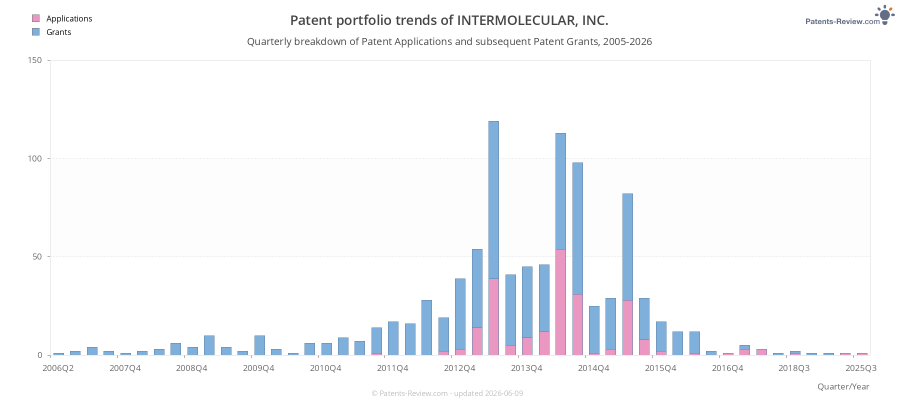
953
2021-06-17
732
2021-10-05
Top Inventors for applications by INTERMOLECULAR, INC.
These are the the leading inventors for applications assigned to INTERMOLECULAR, INC.:
- Tony P. Chiang 144 Campbell, CA United States
- Yun Wang 117 San Jose, CA United States
- Imran Hashim 93 Saratoga, CA United States
- Tony Chiang 84 Campbell, CA United States
- Dipankar Pramanik 75 Saratoga, CA United States
- Minh Huu Le 68 San Jose, CA United States
- Chi-I Lang 63 Cupertino, CA United States
- Prashant B. Phatak 62 San Jose, CA United States
- Intermolecular, Inc. 55 San Jose, CA United States
- Guowen Ding 54 San Jose, CA United States
- Pragati KUMAR 42 Santa Clara, CA United States
- Hiroyuki Ode 41 Higashihiroshima, Japan
- Hanhong Chen 40 Milpitas, CA United States
- Jeroen Van Duren 39 Palo Alto, CA United States
- Jinhong Tong 39 Santa Clara, CA United States
- Haifan Liang 38 Fremont, CA United States
- Prashant Phatak 37 San Jose, CA United States
- Sandra G. Malhotra 37 Fort Collins, CO United States
- Sunil Shanker 37 Santa Clara, CA United States
- Tim Minvielle 36 San Jose, CA United States
- Takeshi Yamaguchi 35 Kanagawa, Japan
- Vidyut Gopal 34 Sunnyvale, CA United States
- Sean Barstow 32 San Jose, CA United States
- Intermolecular, Inc. 30 , United States
- Sandra Malhotra 29 San Jose, CA United States
- Guizhen Zhang 28 Santa Clara, CA United States
- Zhi-Wen Wen Sun 28 Sunnyvale, CA United States
- James Tsung 27 Milpitas, CA United States
- David E. Lazovsky 27 Los Gatos, CA United States
- Wim Deweerd 27 San Jose, CA United States
- Xiangxin Rui 27 Campbell, CA United States
- Kent Riley Child 25 Dublin, CA United States
- Rajesh Kelekar 25 Los Altos, CA United States
- Anh Duong 25 Fremont, CA United States
- Zhi-Wen Sun 25 San Jose, CA United States
- Mihir Tendulkar 24 Mountain View, CA United States
- Sandeep Nijhawan 24 Los Altos, CA United States
- Sergey Barabash 24 San Jose, CA United States
- Hong Sheng Yang 24 Pleasanton, CA United States
- Michael Miller 24 San Jose, CA United States
- Mohd Fadzli Anwar Hassan 24 San Francisco, CA United States
- Frank Greer 23 Pasadena, CA United States
- Nitin Kumar 23 Fremont, CA United States
- Kurt Weiner 23 San Jose, CA United States
- Sandip Niyogi 22 San Jose, CA United States
- Khaled AHMED 21 Anaheim, CA United States
- Chien-Lan Hsueh 20 Campbell, CA United States
- Thomas R. Boussie 20 Santa Clara, CA United States
- Zhi-Wen Sun 20 Sunnyvale, CA United States
- Federico Nardi 19 Palo Alto, CA United States
- Yu Wang 19 San Jose, CA United States
- Randall J. Higuchi 19 San Jose, CA United States
- Sandra G. Malhotra 19 San Jose, CA United States
- Tony P. Chiang 18 San Jose, CA United States
- Sang Lee 18 San Jose, CA United States
- Jeremy Cheng 18 Cupertino, CA United States
- Edward Haywood 18 San Jose, CA United States
- ShouQian Shao 17 Fremont, CA United States
- Brent Boyce 17 Novi, MI United States
- Daniel Schweigert 17 Fremont, CA United States
- Hanhong Chen 17 San Jose, CA United States
- Olov Karlsson 16 San Jose, CA United States
- Aaron Francis 16 San Jose, CA United States
- Chi-I LANG 15 Sunnyvale, CA United States
- Nikhil KALYANKAR 15 Mountain View, CA United States
- Minh Anh Nguyen 15 San Jose, CA United States
- Mankoo Lee 15 Fremont, CA United States
- Wim Y. Deweerd 14 San Jose, CA United States
- John Foster 14 Mountain View, CA United States
- Hieu Pham 13 Santa Clara, CA United States
- Scott Jewhurst 13 Redwood City, CA United States
- Kurt H. Weiner 13 San Jose, CA United States
- Indranil De 13 Mountain View, CA United States
- Yongli XU 13 Plymouth, MI United States
- Venkat Ananthan 12 Cupertino, CA United States
- Thai Cheng Chua 12 Cupertino, CA United States
- Sandra Malhotra 12 Fort Collins, CO United States
- Alexander Gorer 12 Los Gatos, CA United States
- Aaron T. Francis 12 San Jose, CA United States
- Rick Endo 12 San Carlos, CA United States
- Satbir Kahlon 12 Livermore, CA United States
- Ashish Bodke 12 San Jose, CA United States
- David E. Lazovsky 12 San Jose, CA United States
- Alexander Gorer 12 Santa Clara, CA United States
- Nikhil D. Kalyankar 11 Hayward, CA United States
- Amol Joshi 11 Sunnyvale, CA United States
- Hien Minh Huu Le 11 San Jose, CA United States
- Jeffrey Chih-Hou Lowe 11 Cupertino, CA United States
- Philip A. Kraus 10 San Jose, CA United States
- Karthik Ramani 10 Santa Clara, CA United States
- Muhammad Imran 10 Brownstown, MI United States
- Thomas R. BOUSSIE 10 Menlo Park, CA United States
- Charlene Chen 10 San Jose, CA United States
- Zhendong Hong 10 San Jose, CA United States
- Nobumichi Fuchigami 10 Sunnyvale, CA United States
- Wen Wu 10 Pleasanton, CA United States
- Jingang Su 9 Cupertino, CA United States
- Jason Wright 9 Saratoga, CA United States
- Kenichi Koyanagi 9 Higashihiroshima, Japan
- Nitin Kumar 9 Menlo Park, CA United States
Recent patent applications by INTERMOLECULAR, INC.
INTERMOLECULAR, INC. based in San Jose, US has been assigned the rights to these inventions. The list includes both Pending Applications and Patent Grants:
US20210183674A1
ElectricityThin film deposition in a high aspect ratio feature
#2 | 2020-05-14 ✅ Patent 10,833,263 granted on 2020-11-10US20200152867A1
ElectricityCurrent compliance layers and memory arrays comprising thereof
#3 | 2018-09-27US20180277289A1
ElectricityInverse Phase Allotrope Rare Earth Magnets
#4 | 2018-07-12 ✅ Patent 10,580,978 granted on 2020-03-03US20180198064A1
ElectricityCurrent compliance layers and memory arrays comprising thereof
#5 | 2017-08-17 ✅ Patent 10,364,497 granted on 2019-07-30US20170233868A1
Chemistry; metallurgyVapor based site-isolated processing systems and methods
#6 | 2017-06-29US20170186935A1
ElectricityLow Temperature Deposition of Silicon Containing Layers in Superconducting Circuits
#7 | 2017-04-27US20170117282A1
ElectricityDRAM Capacitors and Methods for Forming the Same
#8 | 2017-04-13US20170104031A1
ElectricitySelector Elements
#9 | 2017-03-23US20170084680A1
ElectricityMethods for Forming High-K Dielectric Materials with Tunable Properties
#10 | 2017-03-23US20170084643A1
ElectricityStorage Capacitors for Displays and Methods for Forming the Same
#11 | 2017-03-02 ✅ Patent 9,680,092 granted on 2017-06-13US20170062524A1
ElectricityCurrent selectors formed using single stack structures
#12 | 2017-03-02US20170062522A1
ElectricityCombining Materials in Different Components of Selector Elements of Integrated Circuits
#13 | 2017-02-23 ✅ Patent 9,703,024 granted on 2017-07-11US20170052297A1
PhysicsSystems, methods, and apparatus for production coatings of low-emissivity glass including a ternary alloy
#14 | 2016-10-20US20160304815A1
Chemistry; metallurgyMETHODS AND CHEMICAL SOLUTIONS FOR CLEANING PHOTOMASKS USING QUATERNARY AMMONIUM HYDROXIDES
#15 | 2016-09-27 ✅ Patent 9,455,393 granted on 2016-09-27US14981163
ElectricityLow temperature deposition of low loss dielectric layers in superconducting circuits
#16 | 2016-08-11 ✅ Patent 9,455,437 granted on 2016-09-27US20160233541A1
ElectricitySolid-state batteries utilizing template layers for electrode formation and methods for forming the same
#17 | 2016-06-23 ✅ Patent 9,391,232 granted on 2016-07-12US20160181468A1
ElectricityVariable composition transparent conductive oxide layer and methods of forming thereof
#18 | 2016-06-16 ✅ Patent 9,543,516 granted on 2017-01-10US20160172588A1
ElectricityMethod for forming a doped metal oxide for use in resistive switching memory elements
#19 | 2016-06-09 ✅ Patent 9,425,389 granted on 2016-08-23US20160163977A1
ElectricityDoped ternary nitride embedded resistors for resistive random access memory cells
#20 | 2016-05-26 ✅ Patent 9,786,368 granted on 2017-10-10US20160149130A1
ElectricityTwo stage forming of resistive random access memory cells
#21 | 2016-05-26 ✅ Patent 9,368,721 granted on 2016-06-14US20160149128A1
ElectricityDiamond like carbon (DLC) as a thermal sink in a selector stack for non-volatile memory application
#22 | 2016-05-12US20160133819A1
ElectricityFluorine Containing Low Loss Dielectric Layers for Superconducting Circuits
#23 | 2016-04-28 ✅ Patent 9,337,238 granted on 2016-05-10US20160118440A1
ElectricityPhoto-induced MSM stack
#24 | 2016-04-26 ✅ Patent 9,324,767 granted on 2016-04-26US14145410
ElectricitySuperconducting junctions
#25 | 2016-04-21 ✅ Patent 9,318,531 granted on 2016-04-19US20160111471A1
ElectricitySiC—Si3N4 nanolaminates as a semiconductor for MSM snapback selector devices
#26 | 2016-04-14 ✅ Patent 9,296,650 granted on 2016-03-29US20160102013A1
Chemistry; metallurgyLow-E panels and methods for forming the same
#27 | 2016-04-07 ✅ Patent 9,318,546 granted on 2016-04-19US20160099303A1
ElectricityDoped electrode for DRAM capacitor stack
#28 | 2016-04-07 ✅ Patent 9,482,920 granted on 2016-11-01US20160097945A1
PhysicsTransparent resistive random access memory cells
#29 | 2016-03-01 ✅ Patent 9,276,210 granted on 2016-03-01US14561212
ElectricityConductive barriers for ternary nitride thin-film resistors
#30 | 2016-02-11 ✅ Patent 9,362,231 granted on 2016-06-07US20160042991A1
ElectricityMolecular self-assembly in substrate processing
#31 | 2016-02-04 ✅ Patent 9,607,904 granted on 2017-03-28US20160035631A1
ElectricityAtomic layer deposition of HfAlC as a metal gate workfunction material in MOS devices
#32 | 2016-01-28 ✅ Patent 9,246,091 granted on 2016-01-26US20160028008A1
ElectricityReRAM cells with diffusion-resistant metal silicon oxide layers
#33 | 2016-01-28 ✅ Patent 9,246,085 granted on 2016-01-26US20160028003A1
ElectricityShaping ReRAM conductive filaments by controlling grain-boundary density
#34 | 2016-01-26 ✅ Patent 9,246,092 granted on 2016-01-26US14554458
ElectricityTunneling barrier creation in MSM stack as a selector device for non-volatile memory application
#35 | 2016-01-26 ✅ Patent 9,246,087 granted on 2016-01-26US14551878
ElectricityElectron barrier height controlled interfaces of resistive switching layers in resistive random access memory cells
#36 | 2016-01-26 ✅ Patent 9,246,099 granted on 2016-01-26US14539105
ElectricityLow-temperature deposition of nitrides by UV-assisted ALD or CVD
#37 | 2016-01-19 ✅ Patent 9,240,236 granted on 2016-01-19US14577613
PhysicsSwitching conditions for resistive random access memory cells
#38 | 2016-01-14 ✅ Patent 9,306,126 granted on 2016-04-05US20160013367A1
ElectricityOxides with thin metallic layers as transparent ohmic contacts for p-type and n-type gallium nitride
#39 | 2016-01-05 ✅ Patent 9,231,203 granted on 2016-01-05US14565097
ElectricityDoped narrow band gap nitrides for embedded resistors of resistive random access memory cells
#40 | 2015-12-24 ✅ Patent 9,831,100 granted on 2017-11-28US20150371872A1
ElectricitySolution based etching of titanium carbide and titanium nitride structures
#41 | 2015-12-24 ✅ Patent 9,416,049 granted on 2016-08-16US20150368152A1
Chemistry; metallurgyLow-e panels and methods for forming the same
#42 | 2015-12-03 ✅ Patent 9,224,639 granted on 2015-12-29US20150348833A1
ElectricityMethod to etch cu/Ta/TaN selectively using dilute aqueous Hf/hCl solution
#43 | 2015-12-03 ✅ Patent 9,481,924 granted on 2016-11-01US20150345005A1
Chemistry; metallurgySeed layer for low-e applications
#44 | 2015-11-26 ✅ Patent 9,297,775 granted on 2016-03-29US20150338362A1
PhysicsCombinatorial screening of metallic diffusion barriers
#45 | 2015-11-12 ✅ Patent 9,408,303 granted on 2016-08-02US20150327366A1
ElectricitySilver based conductive layer for flexible electronics
#46 | 2015-11-12 ✅ Patent 9,444,047 granted on 2016-09-13US20150325788A1
ElectricityEmbedded nonvolatile memory elements having resistive switching characteristics
#47 | 2015-11-10 ✅ Patent 9,184,379 granted on 2015-11-10US14335504
ElectricityCapping thin-film resistors to control interface oxidation
#48 | 2015-11-05US20150318446A1
ElectricityLow-Temperature Fabrication of Transparent Conductive Contacts for p-GaN and n-GaN
#49 | 2015-11-03 ✅ Patent 9,177,916 granted on 2015-11-03US14553354
ElectricityAmorphous silicon doped with fluorine for selectors of resistive random access memory cells
#50 | 2015-10-29 ✅ Patent 9,455,073 granted on 2016-09-27US20150313046A1
ElectricitySuperconducting circuits with reduced microwave absorption
#51 | 2015-10-29 ✅ Patent 9,246,062 granted on 2016-01-26US20150311397A1
ElectricityZinc stannate ohmic contacts for p-type gallium nitride
#52 | 2015-10-29 ✅ Patent 9,178,000 granted on 2015-11-03US20150311257A1
ElectricityResistive random access memory cells having shared electrodes with transistor devices
#53 | 2015-10-29 ✅ Patent 9,275,727 granted on 2016-03-01US20150310910A1
PhysicsMulti-level memory array having resistive elements for multi-bit data storage
#54 | 2015-10-22 ✅ Patent 9,196,475 granted on 2015-11-24US20150303057A1
ElectricityMethods for fabricating integrated circuits including fluorine incorporation
#55 | 2015-10-15US20150291812A1
Chemistry; metallurgyLow Emissivity Glass Incorporating Phosphorescent Rare Earth Compounds
#56 | 2015-10-01 ✅ Patent 9,337,030 granted on 2016-05-10US20150279670A1
ElectricityMethod to grow in-situ crystalline IGZO using co-sputtering targets
#57 | 2015-09-22 ✅ Patent 9,142,764 granted on 2015-09-22US14563073
ElectricityMethods of forming embedded resistors for resistive random access memory cells
#58 | 2015-09-10 ✅ Patent 9,276,211 granted on 2016-03-01US20150255716A1
ElectricityNon-volatile resistive-switching memories
#59 | 2015-09-10 ✅ Patent 9,123,785 granted on 2015-09-01US20150255340A1
ElectricityMethod to etch Cu/Ta/TaN selectively using dilute aqueous HF/HCI solution
#60 | 2015-08-20 ✅ Patent 9,331,279 granted on 2016-05-03US20150236260A1
ElectricityCreating an embedded ReRAM memory from a high-k metal gate transistor structure
#61 | 2015-08-20 ✅ Patent 9,315,414 granted on 2016-04-19US20150232378A1
Chemistry; metallurgyLow-e panels with ternary metal oxide dielectric layer and method for forming the same
#62 | 2015-08-20 ✅ Patent 9,321,676 granted on 2016-04-26US20150232376A1
Chemistry; metallurgyLow-E glazing performance by seed structure optimization
#63 | 2015-08-13 ✅ Patent 9,178,006 granted on 2015-11-03US20150228710A1
ElectricityMethods to improve electrical performance of ZrO2 based high-K dielectric materials for DRAM applications
#64 | 2015-08-13 ✅ Patent 9,159,683 granted on 2015-10-13US20150228595A1
ElectricityMethods for etching copper during the fabrication of integrated circuits
#65 | 2015-07-16 ✅ Patent 9,087,978 granted on 2015-07-21US20150200361A1
ElectricityTransition metal oxide bilayers
#66 | 2015-07-09 ✅ Patent 9,410,359 granted on 2016-08-09US20150191965A1
Fixed constructionsLow-e panels and methods for forming the same
#67 | 2015-07-02 ✅ Patent 9,054,634 granted on 2015-06-09US20150188492A1
ElectricityVoltage controlling assemblies including variable resistance devices
#68 | 2015-07-02 ✅ Patent 9,246,097 granted on 2016-01-26US20150188048A1
ElectricityDiffusion barrier layer for resistive random access memory cells
#69 | 2015-07-02 ✅ Patent 9,224,950 granted on 2015-12-29US20150188046A1
ElectricityMethods, systems, and apparatus for improving thin film resistor reliability
#70 | 2015-07-02 ✅ Patent 9,246,094 granted on 2016-01-26US20150188045A1
ElectricityStacked bi-layer as the low power switchable RRAM
#71 | 2015-07-02US20150188044A1
ElectricityEmbedded Resistors for Resistive Random Access Memory Cells
#72 | 2015-07-02 ✅ Patent 9,269,902 granted on 2016-02-23US20150188043A1
ElectricityEmbedded resistors for resistive random access memory cells
#73 | 2015-07-02US20150188039A1
ElectricityEmbedded Resistors with Oxygen Gettering Layers
#74 | 2015-07-02 ✅ Patent 9,431,569 granted on 2016-08-30US20150187982A1
ElectricityZinc blende cadmium—manganese—telluride with reduced hole compensation effects and methods for forming the same
#75 | 2015-07-02US20150187958A1
ElectricityIGZO Devices with Reduced Electrode Contact Resistivity and Methods for Forming the Same
#76 | 2015-07-02US20150187956A1
ElectricityIGZO Devices with Increased Drive Current and Methods for Forming the Same
#77 | 2015-07-02 ✅ Patent 9,224,799 granted on 2015-12-29US20150187865A1
ElectricityCapacitors including inner and outer electrodes
#78 | 2015-07-02US20150187841A1
ElectricityMethod of forming current-programmable inline resistor
#79 | 2015-07-02US20150187664A1
ElectricityHigh Productivity Combinatorial Testing of Multiple Work Function Materials on the Same Semiconductor Substrate
#80 | 2015-07-02 ✅ Patent 9,418,865 granted on 2016-08-16US20150187596A1
ElectricityWet etching of silicon containing antireflective coatings
#81 | 2015-07-02US20150187574A1
ElectricityIGZO with Intra-Layer Variations and Methods for Forming the Same
#82 | 2015-07-02 ✅ Patent 9,297,773 granted on 2016-03-29US20150185170A1
PhysicsX-ray fluorescence analysis of thin-film coverage defects
#83 | 2015-07-02US20150184287A1
Chemistry; metallurgySystems and Methods for Parallel Combinatorial Vapor Deposition Processing
#84 | 2015-07-02 ✅ Patent 9,593,414 granted on 2017-03-14US20150184286A1
Chemistry; metallurgyHydrogenated amorphous silicon dielectric for superconducting devices
#85 | 2015-07-02 ✅ Patent 9,243,321 granted on 2016-01-26US20150184283A1
Chemistry; metallurgyTernary metal nitride formation by annealing constituent layers
#86 | 2015-06-25 ✅ Patent 9,178,152 granted on 2015-11-03US20150179937A1
ElectricityMetal organic chemical vapor deposition of embedded resistors for ReRAM cells
#87 | 2015-06-25 ✅ Patent 9,246,096 granted on 2016-01-26US20150179935A1
ElectricityAtomic layer deposition of metal oxides for memory applications
#88 | 2015-06-25US20150179934A1
ElectricityZrOx/STO/ZrOx Based Selector Element
#89 | 2015-06-25 ✅ Patent 9,443,906 granted on 2016-09-13US20150179933A1
ElectricityTiOx based selector element
#90 | 2015-06-25US20150179930A1
ElectricitySchottky Barriers for Resistive Random Access Memory Cells
#91 | 2015-06-25 ✅ Patent 9,425,376 granted on 2016-08-23US20150179918A1
ElectricityPlasma cleaning of superconducting layers
#92 | 2015-06-25 ✅ Patent 9,281,463 granted on 2016-03-08US20150179917A1
ElectricityAtomic layer deposition of metal-oxide tunnel barriers using optimized oxidants
#93 | 2015-06-25 ✅ Patent 9,082,927 granted on 2015-07-14US20150179916A1
ElectricityCatalytic growth of Josephson junction tunnel barrier
#94 | 2015-06-25US20150179915A1
ElectricityFluorine Passivation During Deposition of Dielectrics for Superconducting Electronics
#95 | 2015-06-25US20150179914A1
ElectricityAnnealed dielectrics and heat-tolerant conductors for superconducting electronics
#96 | 2015-06-25 ✅ Patent 9,297,067 granted on 2016-03-29US20150179913A1
ElectricityFluorine passivation of dielectric for superconducting electronics
#97 | 2015-06-25US20150179839A1
ElectricityCONTACT LAYERS FOR PHOTOVOLTAIC DEVICES
#98 | 2015-06-25US20150179815A1
ElectricityQuantum Well IGZO Devices and Methods for Forming the Same
#99 | 2015-06-25 ✅ Patent 9,082,793 granted on 2015-07-14US20150179773A1
ElectricityIGZO devices with reduced threshhold voltage shift and methods for forming the same
#100 | 2015-06-25 ✅ Patent 9,099,488 granted on 2015-08-04US20150179757A1
ElectricityMethods to characterize an embedded interface of a CMOS gate stack
Also check out Intermolecular, Inc.'s (San Jose, United States) applicant profile with 395 patent applications submitted.
4741 ⎘